|
|||||||||||
|
|
|||||||||||
|
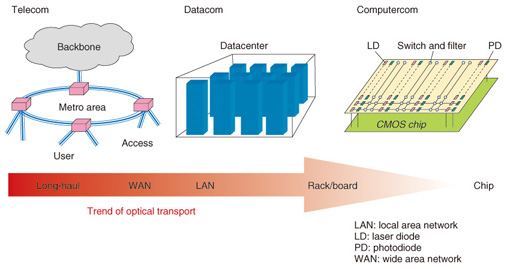
Feature Articles: Optical Semiconductor Technologies for Photonic Networks Vol. 10, No. 12, pp. 62–67, Dec. 2012. https://doi.org/10.53829/ntr201212fa10 Current-injection Photonic-crystal LaserAbstractThis article introduces current-injection photonic-crystal lasers featuring ultralow power consumption, which were achieved by using photonic-crystal nanocavities and small buried active regions fabricated through a crystal regrowth process. They should provide light sources suitable for future lower-power-consumption information and communications technology (ICT) devices.  1. Introduction1.1 Development of photonic networksPhotonic networks have been developed for long-reach optical-fiber communications (telecom). Recently, optical communication technologies have begun to be applied to short-reach data transmission in datacenters (datacom) as optical interconnections between routers and datacenters and between racks and between electronic circuit boards, as shown in Fig. 1. The next challenge is photonic networks for inter-chip and intra-chip transmission (computercom) in microprocessors.
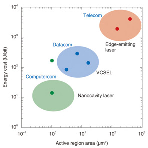
The development has been driven by the explosive growth in information volume on networks including the Internet with the spread of FTTH (fiber to the home), which has increased the need for high-speed information processing at datacenters. Information and communications technology (ICT) devices with large information capacities, high functionality, and high-speed operation have been developed. These ICT devices use electrical data transmission, but the transmission capacity per pin in a microprocessor is limited and an increase in the transmission capacity necessitates greater power consumption. Photonic networks based on wavelength division multiplexing (WDM) are suitable for high-capacity transmission. In addition, the energy consumption per bit is expected to be lower for optical transmission than for electrical transmission for high-speed operation. Therefore, the application of optical interconnection and WDM-based photonic networks to short-reach data transmission has begun to be discussed. 1.2 Optical sources for photonic networksPhotonic networks consist of various kinds of optical devices: the most essential one is a semiconductor laser as a light-emitting device. The relationships between the active region areas of semiconductor lasers and their energy costs are shown in Fig. 2. In general, semiconductor lasers with larger active regions can generate higher output power, but require higher injection current for high-speed modulation and thus have a higher energy cost. For long-reach telecom applications, semiconductor lasers with large active regions are essential because high output power is required. For short-reach applications, on the other hand, semiconductor lasers with small active regions are essential because of the greater need to reduce their energy costs. Vertical cavity surface emitting lasers (VCSELs), which can have shorter cavity lengths and smaller active regions, have recently begun to be applied to datacom applications. However, even VCSELs have limits on how much the active region can be reduced in size. For computercom use, the energy cost of a semiconductor laser should be less than 10 fJ/bit, which requires a semiconductor laser with an active region smaller than 1 µm2, as shown in Fig. 2. Such lasers have not been achieved yet. NTT has focused on photonic crystal, which has the potential to enable the fabrication of semiconductor lasers with tiny cavities and small active regions.
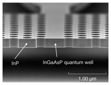
2. Photonic crystalA photonic crystal is an artificial structure whose refractive index is periodically modulated with submicrometer periodicity [1]. A scanning electron microscope (SEM) image of a two-dimensional photonic crystal with periodically placed air holes in the semiconductor slab is shown in Fig. 3. The semiconductor and air have significantly different refractive indices, and their periodic placement in the photonic crystal prevents light of a particular wavelength from existing in the semiconductor. This behavior, which is like a photonic insulator, is a feature of a photonic crystal. If some air holes are removed in a linear fashion (creating a line defect structure) from a two-dimensional photonic crystal with a slab structure, as shown in Fig. 3, then the lightwave can exist in the line defect region. In other words, the line defect acts as a waveguide. In this way, photonic crystals can control lightwaves by the alignment and size of the air holes.
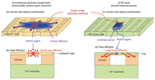
3. Lambda-scale embedded active region photonic-crystal (LEAP) laserVarious photonic-crystal lasers have been reported; however, most of them are fabricated using a horizontally uniform layer slab structure, like InGaAsP MQW (multiple quantum well) with high thermal resistance, as illustrated in Figs. 4(a) and (b). The semiconductor laser needs to confine both light and electrical charge carriers in the active region for lasing. Therefore, ordinary semiconductor lasers have a double-heterostructure, in which the active region is sandwiched by wide-bandgap semiconductors. However, photonic-crystal lasers with a horizontally uniform layer structure can confine only light not carriers because they cannot have a double-heterostructure horizontally against the substrate. Therefore, the lasing characteristics of photonic-crystal lasers with the horizontally uniform layer structure are significantly limited because their performance is adversely affected by carrier diffusion and a temperature rise. To solve these problems, we have utilized a structure with the active region limited to within a line defect in the photonic crystal slab (buried heterostructure) (Figs. 4(c) and (d)). We call this laser the lambda-scale embedded active-region photonic-crystal laser, or LEAP laser for short. Since the refractive index of the active region (InGaAsP- or InGaAlAs-based MQW) is higher than that of the region burying it (InP), the lightwave is strongly confined in the active region. The active region can also confine carriers because its bandgap is smaller than that of the burying region. In addition, the thermal conductivity of InP (68 W/m⋅K) is higher than that of InGaAsP (4 W/m⋅K) and this enables effective heat diffusion (Fig. 4(d)).
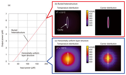
The advantages of the buried heterostructure are shown in Fig. 5. The optical input-output characteristics of optically pumped photonic-crystal lasers using an optical pump wavelength of 0.98 µm and pumping diameter of 4 µm were numerically simulated. In the conventional photonic-crystal laser with the horizontally uniform layer structure, generated carriers spread outside the cavity and the low thermal conductivity causes a significant rise in temperature. Since high temperature degrades the optical properties of the active region, the laser’s resulting output power is low. On the other hand, in a buried-heterostructure laser with an active region of 4 × 0.3 µm2, carriers are strongly confined in the active region and the temperature rise is negligible. Therefore, high output power can be obtained at room temperature. The use of the buried heterostructure is expected to greatly improve the lasing characteristics of photonic-crystal lasers.
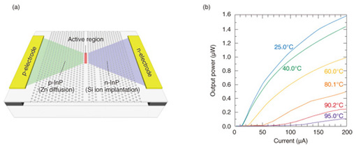
Taking advantage of NTT’s expertise in laser fabrication, especially crystal regrowth techniques for semiconductors, we successfully fabricated the buried-heterostructure active region in the line-defect waveguide in the photonic crystal slab. The size of the active region is 5 × 0.3 × 0.15 µm3. Input and output interfaces are easily fabricated using line-defect waveguides. We have successfully demonstrated optically pumped photonic-crystal lasers operating with power consumption of less than 10 fJ/bit [3]. 4. Current-injection LEAP laserWe made an optically pumped LEAP laser using the buried heterostructure for the first time. However, for practical use in a photonic network, current-injection operation is essential. Current-injection operation of a semiconductor laser requires a pin-junction (p: positive-type semiconductor, i: intrinsic semiconductor, n: negative-type semiconductor). In ordinary lasers, the pin-junction is fabricated in the direction perpendicular to the substrate. Since the LEAP laser needs a slab structure, a pin-junction in the perpendicular direction is difficult to fabricate. We fabricated a pin-junction in the plane of the photonic-crystal slab by using Zn diffusion and Si ion implantation into the non-doped InP burying region. The fabricated current-injection LEAP laser is shown in Fig. 6(a). This is the world’s first current-injection photonic-crystal laser operating with continuous-wave light at room temperature [4]. We achieved a threshold current of 0.39 mA. High-speed modulation at 10 Gbit/s and energy cost of 170 fJ/s were also demonstrated. However, initial devices suffered from a large leakage current, which limited the resulting reductions in threshold current and energy cost despite the active region being small. The origin of the leakage current was the InGaAs etching layer sustaining the air bridge. The small bandgap of InGaAs causes the current leakage. We successfully reduced the leakage current by using InAlAs, which has a larger bandgap than InP, instead of InGaAs for the etching layer. The measured current-light-output curve is shown in Fig. 6(b). Lasing with a very low threshold current of 14 µA was successfully demonstrated at room temperature (25°C). The use of an InGaAlAs-MQW active region enabled high-temperature operation up to 95°C. These figures for low threshold current and high operating temperature are records for photonic-crystal lasers [5].
5. ConclusionThe LEAP laser is a key device for future photonic networks with large capacity and low power consumption. We believe that current-injection LEAP lasers operating with power consumption of less than 10 fJ/bit will be achieved in the near future. We will continue our research and development toward integration of the LEAP laser with silicon photonics and CMOS (complementary metal oxide semiconductor) and ultimately aim at devices integrating microprocessors and photonic networks. References
|
|||||||||||