|
|||||||||||||||||||||||
|
|
|||||||||||||||||||||||
|
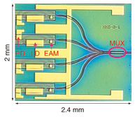
Feature Articles: Optical Semiconductor Technologies for Photonic Networks Vol. 10, No. 12, pp. 45–49, Dec. 2012. https://doi.org/10.53829/ntr201212fa7 Electroabsorption Modulator Integrated Light Sources for Future High-speed EthernetAbstractRecent progress in electroabsorption modulator integrated distributed feedback (EADFB) lasers for high-speed data communications is described. For 100 Gigabit Ethernet (100GbE) applications, an ultrasmall optical semiconductor chip, in which four 1.3-µm 25-Gbit/s EADFB lasers and an optical multiplexer are monolithically integrated, has been developed for future 100GbE transceivers. This small chip enables the overall transmitter size and the number of optical components to be significantly reduced compared with conventional 100GbE transmitters. Furthermore, for future beyond-100-Gbit/s applications, we have developed 50-Gbit/s EADFB lasers and obtained very clear eye openings even after 40-km transmission.  1. IntroductionTo cope with the demand for huge data capacities in local area networks (LANs), 100 Gigabit Ethernet (100GbE) has recently been standardized [1]. In 100GbE, the optical transmitter consists of four 1.3-µm, 25-Gbit/s light sources with a lane spacing of 800 GHz and an optical multiplexer (MUX). So far, work has focused mainly on the development of discrete 25-Gbit/s light sources [2]–[6] for the first-generation transceiver, which is called a centum form-factor pluggable (CFP) transceiver. Since optical components in this transceiver are placed discretely, the size, power consumption, and number of optical components are large. Moreover, since there is a limitation on the transceiver size, reductions in size and power consumption are essential, and these require large-scale-integration of the discrete components. Future high-speed LANs beyond 100 Gbit/s will use a multilane system. Therefore, it is essential to increase the serial data rate of the discrete light source in order to reduce the required number of wavelength lanes, which will lead to smaller transmitters, lower power consumption, and reduced fabrication cost. This article describes recent progress in electroabsorption modulator integrated distributed feedback (EADFB) lasers for high-speed data communications. For 100GbE applications, an ultrasmall optical semiconductor chip [7]–[9], in which four 1.3-µm 25-Gbit/s EADFB lasers and an optical MUX are monolithically integrated, has been developed for future 100GbE transceivers. This small chip enables the overall transmitter size and the number of optical components to be significantly reduced compared with those of conventional 100GbE transmitter. Furthermore, for future beyond-100-Gbit/s applications, we have developed 50-Gbit/s EADFB lasers [10] and obtained very clear eye openings even after 40-km transmission. 2. Monolithically integrated light source for 100GbEA micrograph of the fabricated device is shown in Fig. 1. It consists of four 1.3-µm EADFB lasers and a multimode interferometer (MMI) coupler for the MUX. InGaAlAs-based compressive-strained quantum wells (QWs) are used for the DFB lasers and monitor photodiodes (PDs) and the lasing mode is the transverse electric (TE) mode. To increase the output power of the DFB lasers while retaining single mode lasing, we introduced a novel rear-grating structure [9]. This structure is composed of two sections: one is a conventional l/4 wavelength-shifted grating placed at the rear facet side and the other is just an active region without a grating placed at the front facet side. Both facets are coated with antireflection films. With the active region placed in front of the conventional phase-shifted DFB laser, the lasing mode is amplified in the active region and the longitudinal optical distribution becomes asymmetric, resulting in high output power from the front facet. The design is described in more detail in Ref. [9].
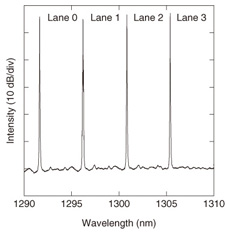
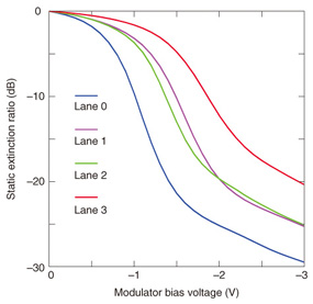
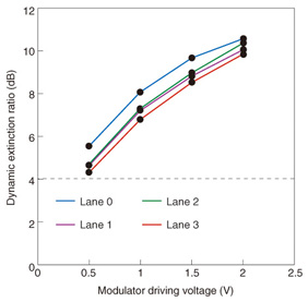
For an electroabsorption modulator (EAM), an effective way to reduce the power consumption of the electrical driver is to reduce the EAM’s driving voltage. To do this, we used InGaAlAs-based, tensile-strained QWs to obtain a large extinction ratio and steep extinction curves [11]. We also made the total thickness of the insulator region small to effectively bias the QW region with low voltage. A shallow-ridge waveguide is buried with benzocyclobutene (BCB) for the EADFB laser section to ensure a large modulation bandwidth. The low dielectric constant of BCB makes the parasitic capacitance lower, and hence the electric/optical (E/O) bandwidth larger. An MMI coupler is used for the MUX because of its small length and low wavelength sensitivity. Deep-ridge waveguides with the InGaAsP-core buried with BCB were used for the MUX region. Since deep-ridge waveguides have stronger optical confinement owing to the large refractive index contrast in the lateral direction, they have low bending and radiation losses compared with shallow-ridge waveguides, leading to a smaller chip size. Metal-organic vapor-phase epitaxy (MOVPE) was used for crystal growth and a butt-joint technique was used to optimize the structures of the DFB laser, EAM, PD, and MUX, separately. The lengths of the DFB lasers, monitor PDs, EAMs, and MMI are 400 µm, 150 µm, 150 µm, and 250 µm, respectively. The width of the MMI is 20 µm. The distance between adjacent EADFB lasers is 600 µm. The fabricated chip is as small as 2.0 mm × 2.4 mm and it is packaged in a specially designed module [8]. The module output power as a function of the injection current to the DFB lasers is shown in Fig. 2. All measurements for the module were done at 40°C. From the shorter wavelength side, we label the wavelength lanes 0 to 3. The output power at the injection current of 150 mA was over 2 mW for all the lanes. The lasing spectra at the injection current of 100 mA are shown in Fig. 3. Single-mode lasing with a side mode suppression ratio of over 50 dB was obtained for all lanes, showing the usefulness of the rear-grating structure for DFB lasers used in monolithically integrated devices. The static extinction curves are shown in Fig. 4. The injection current to the DFB lasers was 100 mA. Static extinction ratios larger than 20 dB as well as steep extinction curves suitable for low-voltage operation were obtained for all lanes. The dynamic extinction ratios of the EAMs as a function of driving voltage (Vpp) are shown in Fig. 5. The bias voltage to the modulator was set at a level where the cross point of the optical eye diagram was 50%. For all lanes, the dynamic extinction ratios were larger than 4 dB, which is the minimum value for 10-km 100GbE (100GBASE-LR4) even with a driving voltage of 0.5 V.
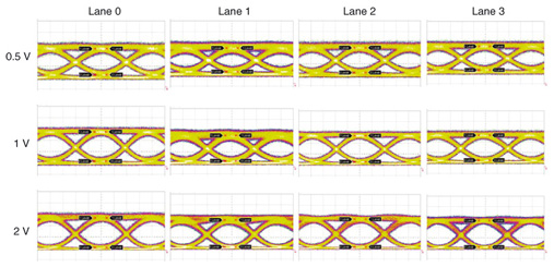
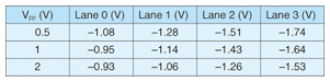
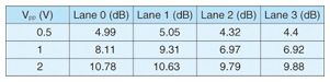
With the module, we performed a 10-km transmission experiment on single-mode optical fiber using a 25-Gbit/s, non-return-to-zero, 231-1 pseudorandom bit stream signal. The eye-diagrams after 10-km transmission with Vpp = 0.5 V, 1 V, and 2 V for all the lanes are shown in Fig. 6. The bias voltages and dynamic extinction ratios to the modulator are summarized in Tables 1 and 2. Clear eye openings were obtained for all driving voltages even after 10-km transmission.
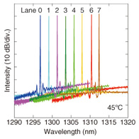
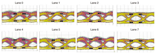
3. EADFB lasers for beyond-100-Gbit/s applicationsFor future high-speed LANs beyond 100 Gbit/s, the serial data rate should be increased to reduce the required number of lanes. Fewer lanes enables reductions in the size, power consumption, and fabrication cost of the whole transmitter. For this purpose, we developed 50-Gbit/s discrete EADFB lasers [10]. The basic structure of the device is described in Refs. [5], [6]. The lasing spectra of the EADFB lasers are shown in Fig. 7. The measurement was done at 45°C. From the shorter wavelength side, we label the lanes 0 to 7. The wavelength spacing is 400 GHz (half of that for 100GbE). The layer structure was the same for all the EADFB lasers. The 50-Gbit/s eye diagrams after 40-km transmission are shown in Fig. 8. The driving voltages were 2 V and the dynamic extinction ratios were larger than 8 dB for all lanes. Very clear eye openings were obtained. Since all the EADFB lasers had the same layer structure, we could integrate them monolithically, as in the case of the 100GbE light source.
4. ConclusionRecent progress in 1.3-µm InGaAlAs-based EADFB lasers for high-speed data communications was described. For 100GbE, an ultrasmall integrated light source was developed. Monolithic integration of the optical components on one chip let us reduce the size of the 100-Gbit/s transmitter chip. This small chip enables us to make small-form-factor 100GbE transceivers. For beyond-100-Gbit/s applications, 50-Gbit/s EADFB lasers were also developed. These devices are promising for future high-capacity data links. References
|
|||||||||||||||||||||||