|
|||||||||
|
|
|||||||||
|
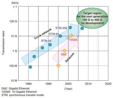
Feature Articles: Circuit and Device Technologies for Extremely Low-power Consumption for Future Communications Systems Vol. 11, No. 2, pp. 18–22, Feb. 2013. https://doi.org/10.53829/ntr201302fa3 Energy-saving Technique for High-speed Packet Forwarding LSIsAbstractNetwork traffic is increasing exponentially, and this requires packet forwarding circuits with higher capacity, which strengthens the demand for higher energy efficiency in these circuits. This article describes an energy-saving technique for high-speed packet forwarding circuits.  1. IntroductionThe packet forwarding circuit in a communication network delivers data from the sender to the recipient. This circuit looks up the media access control (MAC) address (layer 2 switch) and IP (Internet protocol) address (layer 3 switch) that are contained in the inbound packet header and performs a routing function in which it sends the packets to the output ports. NTT Microsystem Integration Laboratories has been carrying out research and development (R&D) on circuit configurations for implementing a next-generation packet forwarding large-scale integrated circuit (LSI). Our research includes high-speed circuit technology for achieving 100-Gbit/s-class packet-forwarding speeds, reduced power consumption, higher performance with the same or lower power consumption, and functional expansion by enabling cooperation between a forwarding LSI and a programmable LSI to allow flexibility in adding future services. Here, we explain our energy-saving technique. 2. Increase in forwarding performance and energy efficiencyResearch efforts are intensifying to achieve faster processing speeds in network devices so they will be able to process the continually increasing amounts of traffic. The forwarding speed at the wavelength of the trunk network is over 100 Gbit/s (Fig. 1) [1]–[3], and the forwarding speed of Ethernet from Datacom Systems is not far behind. The forwarding circuits that route such high-speed packets at the line rate must process a large volume of packets in a very short time. Therefore, either the circuits that implement that function must be operated at a high clock frequency, or the processing must be done by multiple circuits in parallel. Development to suppress the increase in power consumption that comes with these processes is an increasingly important issue from the viewpoint of energy conservation.
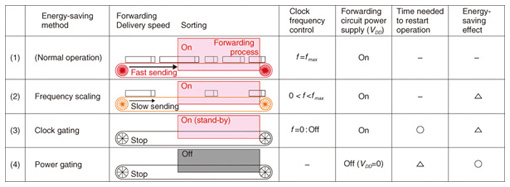
3. Energy-saving methodsThe main approaches to saving energy in LSIs are shown in Fig. 2. These are frequency scaling, in which the frequency of the clock that drives the circuit is lowered, clock gating, in which the clock is periodically stopped, and power gating, in which the power is turned off [4]. The basic principles of these methods when they are applied to packet forwarding can be illustrated through the example of package sorting and delivery. In normal operation, the addresses are sorted and the packages are delivered at high speed. When there are few packages to be delivered, the delivery speed is reduced. When there are no packages to be delivered, the sorting process is put on stand-by, from which it can begin again at any time, and delivery is stopped. The last method is equivalent to stopping both sorting and delivery. In other words, the clock frequency (f) is set to the maximum (fmax) during normal operation to obtain the full performance of the circuit, and the circuit is run on the prescribed power supply (VDD). Frequency scaling conserves energy by reducing the clock frequency (f) according to the amount of processing. As the frequency is lowered, the energy-saving effect increases. Both clock gating and power gating are applied when the amount of processing drops to zero. Clock gating reduces power consumption by stopping the clock signal from being provided to the circuit. Because only the clock is stopped, the circuit remains in stand-by mode, so circuit operation can begin immediately when the clock signal is restored. For that reason, clock gating can be applied for very short time periods, such as in the time interval between packets. However, the power supply (VDD) remains on, so it is not possible to prevent power consumption caused by leakage current, and consequently, the energy-saving effect is not that large. Power gating temporarily or partially stops the power supply. Because power gating can prevent power consumption due to leakage current, it is the most effective of the energy-saving methods. However, once the power is turned off, some time is required to restore it, so this method is applied to circuits that operate for a certain period of time and then stop.
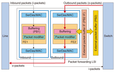
4. Requirements and issuesWhen packets are inbound at 100-Gbit/s-class data rates, the interval between packets is measured in units of nanoseconds (10-9 seconds), so the forwarding circuit must operate constantly. Even when no packets are inbound, the circuit must always remain in a stand-by state that allows immediate forwarding at high throughput when packets arrive without notice. This requirement has made it difficult to apply power gating, which has a recovery time measured in microseconds (10-6 seconds). We therefore developed an energy-saving technique in which power gating is applied by concentrating packets in a packet processing block when throughput is low. We explain that technique in detail below. 5. Power gating techniqueThe basic configuration of a packet forwarding LSI is illustrated in Fig. 3. The functional configuration includes processing of both inbound packets coming from the line (i-packets) and outbound packets going to the line (o-packets). Received packets pass through the serial-parallel converter (SerDes) and the media access controller (MAC) and are buffered and processed for transmission. The packets then pass through the MAC and SerDes and are forwarded. This packet processing sequence is similar for i-packets and o-packets, both in content and procedure, so the two forwarding engines (FE1 and FE2) have approximately the same functions. The i-packet data rate can easily be estimated in advance from the network interface input speed and the number of line ports, but the data rate of the o-packet input from the switch (SW) can fluctuate greatly according to the switching by SW. Therefore, an external packet buffer (PB2) and an interface circuit for it (PB2 IF) are provided so that a packet buffer of appropriate capacity according to the location can be implemented to absorb the data rate fluctuation.
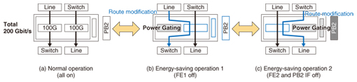
A power gating technique for achieving both high throughput and energy-saving performance when packets are input at short intervals and without notice is illustrated in Fig. 4. During normal operation, the processing of the inbound and outbound packets is done by the respective FEs. The forwarding throughput of each FE is 100 Gbit/s, so forwarding can be done at a total data rate of 200 Gbit/s. However, when traffic is light, the forwarding can be done by just one of the two FEs, and power consumption can be reduced by switching the packet path so that the packets inbound from the line and the packets outbound to the line are both processed by the FE on the right side. In that case, the power to the FE on the left can be turned off to conserve energy (energy-saving operation 1; FE1 off). Furthermore, when traffic is light and the internal packet buffer is sufficient to absorb fluctuations in the data rate, the packets are funneled to the FE on the left side and all packets are processed by that FE. The power to the FE on the right side and the external packet buffer can be turned off to further reduce power consumption (energy-saving operation 2; FE2, PB2, and packet buffer IF are powered off).
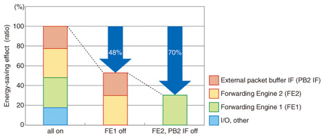
6. Itemized power savingsThe energy-saving effect obtained by applying power gating in which the packet path is changed so that all the forwarding is done by one of the FEs and the power to the other FE is turned off are presented in Fig. 5. The power-gated functional blocks include forwarding engine 1 (FE1), which is off in energy-saving operation 1, forwarding engine 2 (FE2), and the external packet buffer interface (PB2 IF), which are turned off in energy-saving operation 2, and input-output circuits (I/Os), which are off in both energy-saving operations 1 and 2. The energy savings are 48% for energy-saving operation 1, in which one FE and some I/Os are off, and 70% for energy-saving operation 2, in which PB2 IF is also off.
7. ConclusionThe high-throughput packet forwarding LSI is equipped with many high-speed input-output circuits for receiving and forwarding at high data rates and various MAC processing circuits for flexibly handling a variety of protocols. We intend to expand our energy-saving efforts beyond the results shown in Fig. 5 to include those other constituent elements to achieve even further energy savings. References
|
|||||||||