|
|||||
|
|
|||||
|
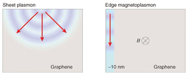
Feature Articles: Front-line Research on Graphene Vol. 11, No. 8, pp. 26–28, Aug. 2013. https://doi.org/10.53829/ntr201308fa5 Plasmon Transport in GrapheneAbstractThis article describes time-resolved measurements of plasmon transport in graphene. It is demonstrated that the plasmon velocity can be varied over two orders of magnitude by changing the magnetic field, carrier density, and the gate screening effect.  1. IntroductionOptical interconnections have the advantages of low-loss and high-speed data transmission over electrical interconnections, and consequently, optical fibers have replaced the metal cables formerly used for short-distance connections between racks and boards in supercomputers as well as for long-distance transmission over the Internet. Furthermore, many research efforts have recently been directed at controlling optical signals and replacing some electronic devices with optical ones, with the aim of further reducing the power consumption. However, the integration of optical devices into electronic chips has been hampered by the diffraction limit of light, which is typically 1000 nm. One possible way to solve this problem is to confine optical signals to nanoscale regions in the form of plasmons. This field of research is called plasmonics, and it is being actively studied, mainly using surface plasmons on metal surfaces. However, there are fundamental limitations to using metals in plasmonics. Namely, the properties of surface plasmons are fixed by the material and the geometry. Furthermore, the loss during the propagation of plasmons is large. NTT Basic Research Laboratories has been investigating plasmons in graphene, where tunable properties and low-loss transport of plasmons are expected. There are two kinds of plasmons in graphene (Fig. 1). One is called a sheet plasmon, which propagates in the two-dimensional plane. The other is called an edge magnetoplasmon (EMP), which appears only in high magnetic fields. EMPs propagate along the sample edge.
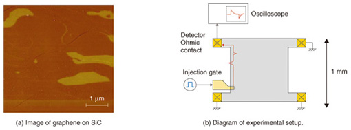
2. Methods of plasmon measurementIn this work, we carried out time-resolved measurement of plasmon transport in graphene. The device structure and the experimental setup are shown in Fig. 2. The graphene used was obtained by thermal decomposition of a silicon carbide (SiC) substrate. The devices are about 1 × 1 mm2 and have four Ohmic contacts. The surfaces of the devices were covered with 100-nm-thick hydrogen silsesquioxane (HSQ) and 40-nm-thick silicon dioxide (SiO2) insulating layers. We used two samples, one with and the other without a large top gate.
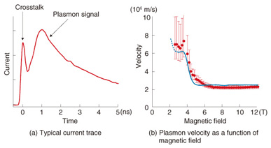
For the time-resolved transport measurement, a pulsed plasmon is generated in graphene by applying a voltage step to the injection gate deposited across the sample edge. The plasmons propagate in graphene and are detected as a time-dependent current through the detector Ohmic contact using a sampling oscilloscope. The plasmon velocity can be determined by measuring the time of flight of plasmons at a time resolution of 100 ps. Although all data shown here were taken at 1.5 K in order to investigate the physics of plasmon transport in detail, we confirmed that the plasmon signal does not change much even at much higher levels, for example, up to several ten K. 3. Effects of magnetic field on plasmon transportA typical current trace is shown in Fig. 3(a). The origin of the time corresponds to the time when plasmons are injected. The sharp peak is due to crosstalk between injection and detection high-frequency lines. Since the crosstalk propagates with the speed of light, it appears with virtually zero time delay. The broader peak that appears with a time delay of about 1 ns is the plasmon signal. The time delay of the plasmon signal from the crosstalk roughly corresponds to the time of flight of plasmons. The plasmon velocity is obtained from the time of flight and the path length.
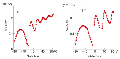
The plasmon velocity in the ungated sample as a function of the magnetic field is shown in Fig. 3(b). The velocity is about 6000 km/s at 3 T and decreases to 2000 km/s as the magnetic field increases. This behavior can be well reproduced theoretically for EMPs (blue trace). For the magnetic field lower than 2 T, the plasmons are too fast and the velocity cannot be determined accurately. This indicates that the plasmon velocity around zero magnetic field is above the maximum measurable value of 6000 km/s. 4. Effects of carrier density and the gate screening effect on plasmon transportThe plasmon velocity in the gated sample as a function of the gate bias at magnetic fields of 8 and 12 T is shown in Fig. 4. The velocity is about 100 km/s, which is one order of magnitude smaller than that in the ungated sample. The smaller velocity is due to the gate screening effect. When there is a metal gate close to the graphene, the electric field in plasmons is partially screened, which reduces the velocity. As the gate bias and thus the electron density decrease, the velocity decreases to several ten km/s with oscillations. This behavior can also be qualitatively explained by EMP theory.
In summary, the velocity of plasmons in graphene can be tuned over a wide range from several ten to thousand km/s by changing the magnetic field, carrier density, and the gate screening effect. The tunability of the velocity indicates the tunability of the refractive index and the impedance. By controlling these parameters, it would be possible to develop plasmonic devices with functionalities such as plasmon switching, guiding, and routing. This work was a collaboration between NTT Basic Research Laboratories and Tokyo Institute of Technology. 5. Future workNTT Basic Research Laboratories has succeeded in controlling the plasmon velocity in graphene over two orders of magnitude. We will try to exploit this result in order to control the plasmon transport. Furthermore, we will estimate the loss of the plasmon signal during the propagation, which is expected to be much smaller than that in metallic systems. References
|
|||||