|
|||||||||||||||||||||||||
|
|
|||||||||||||||||||||||||
|
Feature Articles: Front-line Research on Graphene Vol. 11, No. 8, pp. 29–34, Aug. 2013. https://doi.org/10.53829/ntr201308fa6 Surface-enhanced Raman Scattering of Graphene on SiCAbstractRaman scattering spectroscopy is a well-known optical tool for identifying the properties of graphene such as the number of layers, carrier concentration, and strain. Interaction between incident light and a metallic nanoparticle such as gold or silver enhances the intensity of light, which can be used in Raman scattering spectroscopy. This article describes our investigation of graphene properties by using surface-enhanced Raman scattering.  1. IntroductionGraphene can be grown on a silicon carbide (SiC) substrate by sublimating silicon (Si) in a high-temperature furnace. The use of high-quality and large-area graphene on SiC has enabled a high-frequency transistor and a metrological resistance standard based on the quantum Hall effect*1 to be demonstrated. The interaction between graphene and SiC modifies the graphene carrier concentration and strain, which are basic properties for electronic devices. An electron in strained graphene behaves as if it is in a magnetic field. Strain, along with carrier concentration, is therefore a prominent property of electronic devices. Raman scattering is a non-destructive method for examining these properties. However, the Raman spectrum of SiC is superimposed on the salient spectrum of graphene, which makes it difficult to analyze the graphene's properties. Here, we explain how surface-enhanced Raman scattering (SERS) enhances only the graphene spectrum and thereby makes it possible to quantitatively analyze the Raman spectrum of graphene on SiC.
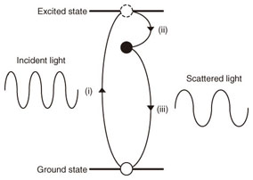
2. Raman scattering and Raman peaks of grapheneIn Raman scattering, the energy of light scattered from a substance is slightly different from that of the incident light. A schematic view of Raman scattering is shown in Fig. 1. The process involves (i) the excitation of electrons from a ground state, (ii) the scattering of the excited electrons with energy relaxation driven by a lattice vibration, and (iii) the transition of the scattered electrons to the ground state and the emission of scattered light. The energy difference between the incident and scattered light is called a Raman shift, which is expressed in an energy unit of cm–1. The energy of the lattice vibration in a material is derived from the Raman shift. Furthermore, electron states can be examined because both an electron and a lattice vibration are related to Raman scattering. The ratio of Raman scattered light to total scattered light is extremely small, and most of the scattered light is Rayleigh scattered light whose energy is the same as that of the incident light. Nonetheless, Raman scattering spectroscopy is a powerful tool for identifying material properties such as the lattice vibration and electron state.
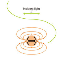
Here, we explain the origin of the salient Raman peaks of graphene on SiC. G (~1600 cm–1) and D (~1350 cm–1) peaks are observed in carbon materials. The D peak originates from defects and bindings to other materials (including carbon). The D' peak (~1630 cm–1) is also due to defects and bindings and is smaller than the G and D peaks. The 2D peak (~2710 cm–1) with a Raman shift nearly twice that of the D peak is observed in graphene without defects and bindings. The 2D intensity decreases as the density of defects and bindings increases. 3. Enhancement of light intensity due to localized surface plasmon resonanceThe interaction between incident light and a metallic nanoparticle such as gold or silver enhances the light intensity in a small region near the nanoparticle, which is illustrated in Fig. 2. Incident light induces polarization in a metallic nanoparticle. The polarization generates an electric field outside the metallic nanoparticle, which can be derived by solving the electric-field equation with the boundary condition of the nanoparticle's spherical surface. The generated electric field is equivalent to the electric field induced by an electric dipole*2 in the center of the nanoparticle. The difference between the air and metal dielectric constants, which depends on the wavelength, results in a remarkable phenomenon: in a resonance with an appropriate wavelength, i.e., localized surface plasmon*3 resonance (LSPR), the electric dipole induces a strong electric field compared with the electric field of the incident light. The LSPR for gold and silver occurs in the visible light range (380–800 nm), and many applications exploiting LSPR have been developed because of its ability to greatly enhance the light intensity. Nanometer-scale metallic nanoparticles exhibit LSPR, and the intensity of the enhanced light decreases rapidly as the distance from the nanoparticles increases. The light enhancement only occurs in a region equivalent to the size of the metallic nanoparticle.
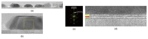
4. Sample fabrication and transmission electron microscopy imageSilver (Ag) nanoparticles were deposited on graphene by Ag evaporation in a high-vacuum chamber*4. The deposited Ag stays in the form of particles rather than forming a layer because of the inertness of graphene. These particles can move and they combine to form aggregate particles about 10 nm in size. A transmission electron microscopy*5 (TEM) image of hemispherical Ag nanoparticles on graphene is shown in Fig. 3(a). The magnified image in Fig. 3(b) shows that there is no damage to the graphene even though Ag was directly deposited on it. We first investigated the structure of crystallized Ag nanoparticles on graphene. In Fig. 3(c), a Fourier transform*6 image of the yellow square in Fig. 3(b) is displayed with the corresponding reciprocal lattice vector of a point that represents the distance of a lattice plane. It is clearly seen that the (111) plane of Ag (face-centered cubic) attaches to the graphene, which is reasonable by considering the lattice constants of Ag and graphene. A magnified image at the interface between an Ag nanoparticle and graphene is shown in Fig. 3(d), where yellow, red, and green lines indicate Ag, graphene, and a buffer layer (a non-conductive carbon layer between the graphene and SiC, where a carbon atom binds to the SiC). We measured the distance between an Ag nanoparticle and the graphene from the TEM image and averaged the distance measured at many points to obtain a distance of 3.14 ± 0.13 Å. By considering a theoretical calculation that the distance is 3.33 Å for physisorption and less than 2.3 Å for chemisorption [1], we conclude that Ag nanoparticles attach to graphene without chemical bonds, i.e., in a physisorbed state, which is consistent with there being no degradation of the graphene under the nanoparticles.
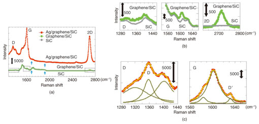
5. Surface-enhanced Raman scattering of graphene on SiCWithout the Ag deposition, the SiC peaks overwhelm the graphene feature of D and G peaks as shown in Fig. 4(a). Enlarged plots of the D, G, and 2D peaks of graphene without Ag nanoparticles are shown in Fig. 4(b). Although there is no SiC peak around the 2D peak of graphene, the SiC peak is superimposed on the graphene D and G peaks, which makes quantitative analysis difficult. With the Ag deposition, the spectrum of graphene with Ag nanoparticles (red) overwhelms that of the SiC substrate (gray). A comparison of the signals of graphene with Ag nanoparticles (red) and without them (green), shows that the enhanced signal of graphene with Ag nanoparticles exhibits clear graphene features of D, G, and 2D peaks. By comparing the 2D peak intensity of graphene with and without Ag nanoparticles, we obtain a nominal enhancement of 37. The large enhancement paves the way to quantitatively analyzing the D and G peaks of graphene on SiC as shown in Fig. 4(c). Sub-peaks at 1320 and 1400 cm–1 are observed in addition to the main D peak at 1360 cm–1. Our SERS method reveals the sub-peak structure, which cannot be resolved in conventional Raman spectroscopy. The G peak also has a sub-peak structure at 1580 cm–1 below the most prominent peak at 1600 cm–1. Furthermore, the D' peak is observed at 1630 cm–1. The peaks at 1580 and 1600 cm–1 are graphene peaks, not SiC peaks. We know this because those peaks are observed in micromechanically cleaved graphene*7 on a Si substrate [2]. As shown in the graph, three-curve fitting is applied to the spectrum around the G peak. The yellow curves represent the summation of the three fitting curves, and the yellowish-brown ones represent each fitting curve.
The D and D' peaks, which are caused by disorder, are observed in graphene with Ag nanoparticles. We attribute them to defects or the buffer layer that was originally present in our sample because no damage is found in the TEM images. Quantitative analysis of the D, D', and G peaks makes it possible to assess disorder in graphene. The peak intensity ratio of D to G and that of D' to G are obtained from the fitting, and they are an order smaller than those of nanocrystalline graphene [3]. Our SERS technique is a powerful method for analyzing the D and G peaks of graphene on SiC and resolving the sub-peak structures, which cannot be observed in conventional Raman spectroscopy.
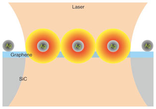
6. Doping effectThe Ag deposition has a doping effect on graphene, which can be estimated by SERS. The carrier density of graphene is derived from the peak intensity ratio of 2D to G [4]. An electron density of 1.9 × 1013 cm–2 is obtained for graphene with Ag nanoparticles. Using an electrical measurement, we estimated a typical electron density of approximately 1 × 1012 cm–2 for graphene without Ag nanoparticles. Our results are consistent with a theoretical calculation that shows Ag-deposited graphene is electron-doped [1]. Care should be taken in estimating the SERS enhancement because the 2D peak intensity decreases as the carrier density increases [5]. By considering the doping effect due to the Ag deposition, the nominal enhancement of 37 is modified to the actual enhancement of approximately 100. The estimation of the correct enhancement is obtained by quantitatively analyzing the electron density of graphene. 7. Enhancing only the graphene signalThe enhancement of only the graphene signal is what makes the quantitative analysis possible. The graphene spectrum is enhanced, while the SiC spectrum is suppressed. The SiC spectrum with Ag nanoparticles becomes around half that without Ag nanoparticles, which is clearly seen in the two peaks at 1700 cm–1 and the shoulder at 1930 cm–1 as indicated by the blue arrows in Fig. 4(a). The light incident to SiC and the light scattered from it are blocked by the Ag nanoparticles. Furthermore, the small region of enhanced light due to LSPR has an impact on the observed phenomenon, as shown in Fig. 5. The region of enhanced light is on the order of the size of the Ag nanoparticles, i.e., 10 nm; therefore, the observed region is also 10 nm in depth. The spot size of the laser in our experiments was 1 µm, and the observed region without Ag nanoparticles was 1 µm in depth. Here, we consider the volume of graphene (monolayer) to the observed region. The volume with Ag nanoparticles is monolayer in 10 nm, and that without them is monolayer in 1 μm, respectively. The volume of monolayer graphene to the observed region with Ag nanoparticles was 100 times larger than that without them. Consequently, our SERS method makes it possible to enhance only the graphene signal efficiently.
8. Further studyIn this article, we showed that the sub-peak structure of the D and G peaks of graphene on SiC with Ag nanoparticles can be revealed using SERS. Thanks to the efficient enhancement of only the graphene signal, the carrier concentration can be obtained by quantitatively analyzing the graphene peaks. We plan to use our SERS technique to estimate the strain due to the interaction between graphene and SiC. The buffer layer between graphene and SiC has an impact on the strain in graphene, and it is removed by high-temperature annealing in a hydrogen atmosphere. We will also investigate the difference between the strain in graphene with and without the buffer layer. Our SERS technique is therefore effective for quantitatively obtaining the basic properties of graphene on SiC. References
|
|||||||||||||||||||||||||