Regular Articles
Vol. 11, No. 8, pp. 40–47, Aug. 2013. https://doi.org/10.53829/ntr201308ra1
1. Introduction
Quantum entanglement, or in other words, nonlocal quantum correlation between two or more quantum-mechanical objects, is a quintessential feature of quantum mechanics. At the same time, quantum entanglement is a substantial resource for quantum information processing (QIP) technologies including quantum cryptography, quantum metrology, and quantum computation [1]–[4].
A number of physical systems are being investigated for their potential application in the development of QIP. Among them, photons are excellent media to generate, process, and distribute entanglements. This is because quantum states encoded in physical quantities of light are highly robust, thanks to an inherent weakness in the interactions between light and electromagnetic environments. The physical freedom of light includes polarizations, optical paths, frequencies, and time bins. Of these quantum states, polarization is particularly important, since polarization is a true two-level photonic system, which is easy to manipulate with conventional bulk optics such as wave plates. Thus, many QIP protocols have been proposed [3], [5] and experimentally demonstrated [4], [5] using polarization-encoded quantum states of light. In such experiments, sources of polarization-entangled photons have been inevitably playing a key role [6], [7].
Very recently, integrated optical circuits have been attracting much attention as the next platform of QIP using photons [8]. Such an approach promises to scale up the experiments by exploiting the miniature physical size and highly stable interferometers of integrated waveguides. To achieve such integrated photonic QIP systems, it is essential to develop integrated subsystems to generate, manipulate, and measure the quantum states on a chip. In particular, an integrated polarization-entanglement source, which generates polarization-entangled photons into a waveguide mode on a chip, is necessary in order for us to utilize the wealth of QIP protocols. However, no such demonstration of an integrated polarization-entanglement source has been reported to date; nevertheless, it is necessary for a practical integrated QIP system. In this article, we present the world’s first ever polarization-entanglement source, which NTT achieved using silicon photonics technology [9] (Fig. 1). We have implemented the source as a simple and stable silicon-on-insulator photonic circuit so the source could successfully generate a high degree of polarization entanglement.
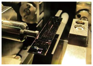
Fig. 1. Picture of the chip of monolithic polarization-entangled photon pair sources. By injecting pump pulses from the left hand side, we can obtain polarization-entangled photon pairs to be collected by the output optical fiber on the right hand side.
2. Building blocks of polarization-entangled photon pair source
An entangled photon pair source requires two building blocks: a source to generate photon pairs having a time correlation, and a device to manipulate the polarization state of photons to ensure that photon pairs are entangled in the polarization degree of freedom. NTT has already realized both components by using on-chip silicon photonics technology.
A silicon-wire waveguide is a highly efficient source of time-correlated photon pairs (Fig. 2(a)) [10]–[15]. The silicon-wire waveguide is a single-mode waveguide whose core is made of single-crystalline silicon with a typical cross-sectional size of 400 nm (width) and 200 nm (height). Thanks to this extremely small core, the optical power density in the waveguide becomes very high, and as a result, we can observe a huge nonlinear optical effect. The nonlinear coefficient of our silicon-wire waveguide is five orders of magnitude larger than that of a silica optical fiber. This coefficient represents the optical-nonlinearity strength of a waveguide.
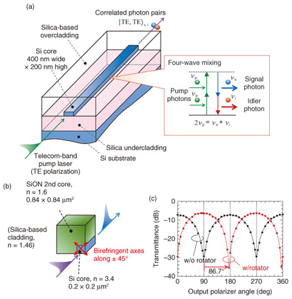
Fig. 2. Building blocks of polarization-entanglement source. (a) Silicon-wire waveguide source of correlated photon pairs. (b) Ultrasmall silicon polarization rotator. Claddings are not shown for clarity. (c) Characterization of polarization rotation angle at the silicon polarization rotator.
When we input a telecom-wavelength pump light whose frequency is νp into the silicon-wire waveguide, we can generate a photon pair with frequencies of νs and νi through spontaneous four-wave mixing (SFWM), which is one of the third-order nonlinear effects. The process occurs under the energy conservation of photons as follows
 This indicates that two pump photons are annihilated, and subsequently a signal-idler photon pair is created. Since the two photons are created simultaneously, we can generate time-correlated photon pairs. In addition, the use of the single-crystalline silicon core enables us to avoid background noise photons caused by spontaneous Raman scattering, which has been a serious problem for photon pair sources based on other types of nonlinear waveguides such as fused silica [1] whose core has an amorphous structure. A single-mode waveguide supports two propagating modes with orthogonal polarization states of light: transverse-electric (TE) and transverse-magnetic (TM) fields. In the silicon wire waveguide, TE-polarized photon pairs are efficiently generated by a TE-polarized pump field. This is because the waveguide has a field confinement of TE-polarized light into the core that is stronger than that of TM-polarized light [13].
The second building block is a silicon polarization rotator [16], which is used in polarization-diversity optical circuits for telecommunication applications [17]. The device has an off-axis double-core structure consisting of a 200-nm2 silicon wire core and a second 840-nm2 silicon-oxynitride (SiON) core on the silicon core (Fig. 2(b)). The structure exhibits two orthogonal eigenmodes, which have different effective refractive indices and eigen-axes tilted at 45° to the normal with respect to the silicon substrate. The birefringence in the eigenmodes provides an integrated wave plate, which causes the polarization plane to rotate by an amount that depends on the length of the rotator. We show the measured polarization rotation characteristics of a 30-μm-long polarization rotator in Fig. 2(c). A TE-polarized input field was successfully converted to TM polarization with the rotator. The polarization rotation angle was estimated to be 86.7 ± 0.1° with a polarization extinction ratio as high as 30 dB. Thus, we obtained a polarization rotation angle of almost 90° with a high polarization extinction ratio. This high performance of the rotator enabled us to generate a high degree of polarization entanglement as we show later.
3. On-chip polarization-entanglement source
We combined the two building blocks fabricated on the same silicon photonics platform to implement the monolithic polarization entanglement source on a chip [9]. Our polarization-entanglement source (Fig. 3) consists of two silicon-wire waveguides connected by a silicon-wire polarization rotator. Both silicon wire waveguides are 1.5 mm long. The silicon wire waveguides and the silicon polarization rotator are connected by 10-μm-long tapered silicon wires. The over- and under-cladding of the silicon wire waveguides and the silicon polarization rotator were made of silica (not shown).
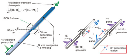
Fig. 3. Monolithically integrated polarization-entangled photon pairs. The source, fabricated on a silicon-on-insulator substrate, consists of a silicon 90° polarization rotator sandwiched by two nonlinear silicon wire waveguides. The device generates the polarization entanglement as a superposition of the two events shown on the right hand side.
The operating principle of the device is as follows. We use a pump beam with + 45° linear polarization, which is a 1:1 combination of the TE and TM modes in the silicon wire waveguides. In the first silicon wire waveguide, the TE component of the pump creates a photon pair in the  state, which means that there is one TE-polarized photon in the signal frequency channel and one TE-polarized photon in the idler frequency channel. In the following, we rewrite the state as state, which means that there is one TE-polarized photon in the signal frequency channel and one TE-polarized photon in the idler frequency channel. In the following, we rewrite the state as  for simplicity. Then, the silicon polarization rotator rotates this state to the for simplicity. Then, the silicon polarization rotator rotates this state to the  state as a result of 90° polarization rotation. Here, the subscripts denote the frequency modes of the signal and idler photons. At the same time, the silicon polarization rotator rotates the TM component of the pump field to provide it with TE polarization, and the second silicon wire waveguide creates other photons. Since we cannot distinguish whether the pair was generated in the first or second silicon waveguides, we obtain the maximally polarization-entangled state: state as a result of 90° polarization rotation. Here, the subscripts denote the frequency modes of the signal and idler photons. At the same time, the silicon polarization rotator rotates the TM component of the pump field to provide it with TE polarization, and the second silicon wire waveguide creates other photons. Since we cannot distinguish whether the pair was generated in the first or second silicon waveguides, we obtain the maximally polarization-entangled state:
 at the output of the polarization-entanglement source. Here, the relative phase difference φ is a fixed value and depends on the difference in length between the first and second silicon waveguides.
Generally, it is difficult to precisely control a birefringence of nonlinear waveguides with an ultrasmall core. The residual birefringence causes significant polarization-mode dispersion (PMD), which degrades the degree of polarization entanglement. To avoid this degradation, the conventional polarization-entanglement sources adopt off-chip PMD compensators such as birefringent crystal or polarization-maintaining fiber. In those cases, photons cannot be polarization-entangled inside the waveguide chip. In our case, since the polarization-entanglement source is designed to be symmetric about the polarization states with respect to the midpoint of the device, the polarization-mode dispersion of the pump pulses and photon pairs are completely cancelled out. Therefore, our polarization-entanglement source generates a polarization-entangled state inside the waveguide chip. This feature enables us to directly integrate the source with quantum-state controllers and detectors to construct a quantum information processor on a chip. Moreover, the device can automatically balance the amplitude of the two terms in Eq. (2) even in the presence of practical waveguide losses, leading to highly robust polarization entanglement (see Ref. [9] for details).
4. Experiment
We generated and analyzed polarization-entangled photon pairs using the setup shown in Fig. 4. We injected optical pump pulses whose polarization was set at + 45° linear polarization and a wavelength centered at 1551.1 nm into the polarization-entanglement source. The photons generated from the chip were introduced into the wavelength-division-multiplexing (WDM) filter, which suppressed the residual pump light and separated the signal and idler photons into different fiber channels. Each output port had a center wavelength of 1546.4 nm (signal) and 1556.0 nm (idler) with a channel bandwidth of 0.14 nm. Then, the photons passed through the polarization analyzers, each of which consisted of a half and a quarter wave plate, and a polarizer. Finally, the photons were received by InGaAs (indium/gallium/arsenide) single photon detectors. The detection signals from the two detectors were input into the time interval analyzer (TIA), with which we carry out time-correlation measurement of photon pairs.
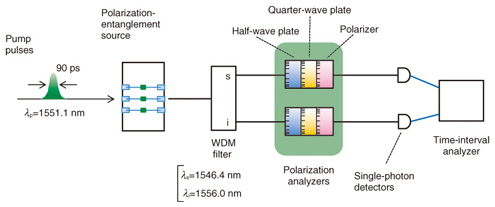
Fig. 4. Experimental setup.
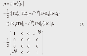
We first reconstruct the density matrix of the generated polarization-entangled state to evaluate the degree of entanglement. The density matrix ρ of the state in Eq. (2) can be expressed as
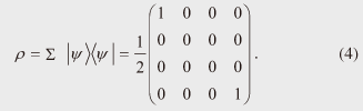
when the state is purely in the maximally entangled state. Here, the summation takes over all the generated photon pairs. In this representation, we used   and as a basis set. Each diagonal element represents the probability (population) of the system, and the off-diagonal elements represent the quantum coherence. If the generated system has no coherence, the density matrix becomes and as a basis set. Each diagonal element represents the probability (population) of the system, and the off-diagonal elements represent the quantum coherence. If the generated system has no coherence, the density matrix becomes
Therefore, the density matrix that has the off-diagonal elements whose absolute values are as high as those of the diagonal elements shows the full coherence of the entanglement.
To experimentally obtain the density matrix of the two-photon polarization state, we first carried out the correlation measurement of the photon pairs under 16 different polarization combinations that were selected based on the angles of the four wave plates in the polarization projection units [18]. This is analogous to the measurement of the polarization state of classical light, in which projection measurements of four different polarization states are at least required to estimate Stokes vectors. In the present case with the two-photon state, we require 42 = 16 projection measurement. Then, using a procedure called quantum state tomography, we can reconstruct the density matrix. The reconstructed density matrix is shown in Fig. 5. For simplicity, we have only displayed the absolute values of each matrix element. The result exhibits off-diagonal amplitudes as high as 0.5, which represent a high coherence of the system. Note that the results include any background (noise) counts.
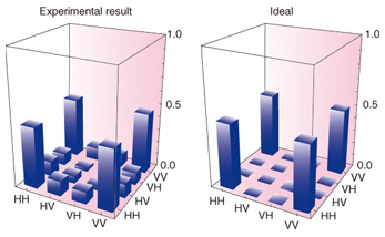
Fig. 5. Reconstructed density matrix. Here, the absolute values of each element are shown. H and V represent the TE and TM bases, respectively.
Regarding the degree of entanglement, we evaluate the fully entangled fraction  where the maximum is taken over all maximally entangled states |Ψ>. From the measured ρ values in accordance with the procedure described by Badziag et al. [19], we obtained an F(ρ) value of (94 ± 2)%. This value is much higher than the classical limit of 0.5. Furthermore, the F(ρ) value is much greater than 1/√2~ 71%, implying that the generated state has strong nonlocal correlation. Hence, we successfully generated photon pairs with a high degree of polarization entanglement from the chip. where the maximum is taken over all maximally entangled states |Ψ>. From the measured ρ values in accordance with the procedure described by Badziag et al. [19], we obtained an F(ρ) value of (94 ± 2)%. This value is much higher than the classical limit of 0.5. Furthermore, the F(ρ) value is much greater than 1/√2~ 71%, implying that the generated state has strong nonlocal correlation. Hence, we successfully generated photon pairs with a high degree of polarization entanglement from the chip.
5. Conclusion
We have demonstrated the world’s first ever source of polarization-entangled photon pairs on a chip. The device we constructed is capable of generating a high degree of polarization entanglement thanks to nanofabrication technology of silicon photonic devices. To achieve a photonic QIP system on a chip, it is necessary to integrate our source with subsequent quantum processors, which manipulate or project the polarization-encoded quantum state of photons. Such integration would also be possible, since our source is equipped with spot-size converters, which can be a versatile interface with other types of integrated waveguide platforms [20]. Our monolithic polarization-entangled photon pair source helps pave the way to the full-scale implementation of a photonic quantum information system on a chip.
References
| [1] | H. Takesue, “Generation of Polarization-entangled Photon Pairs in 1.5-μm Telecommunication Band,” NTT Technical Review, Vol. 3, No. 12, 2005.
https://www.ntt-review.jp/archive/ntttechnical.php?contents=ntr200512052.pdf |
|---|
| [2] | K. Edamatsu, “Entangled Photons: Generation, Observation, and Characterization,” Japan. J. of Appl. Phys., Vol. 46, pp. 7175–7187, 2007. |
|---|
| [3] | M. A. Nielsen and I. L. Chuang, “Quantum Computation and Quantum Information,” Cambridge University Press, Cambridge, 2000. |
|---|
| [4] | H. Takesue, “Quantum Communication Using Entangled Photon Pairs––Toward Quantum Repeaters,” NTT Technical Review, Vol. 9, No. 9, 2011.
https://www.ntt-review.jp/archive/ntttechnical.php?contents=ntr201109fa10.html |
|---|
| [5] | P. Kok, W. J. Munro, K. Nemoto, T. C. Ralph, J. P. Dowling, and G. J. Milburn, “Linear Optical Quantum Computing with Photonic Qubits,” Rev. Mod. Phys., Vol. 79, No. 1, pp. 135–174, 2007. |
|---|
| [6] | P. G. Kwiat, K. Mattle, H. Weinfurter, A. Zeilinger, A. V. Sergienko, and Y. Shih, “New High-Intensity Source of Polarization-Entangled Photon Pairs,” Phys. Rev. Lett., Vol. 75, No. 24, pp. 4337–4341, 1995. |
|---|
| [7] | P. G. Kwiat, E. Waks, A. G. White, I. Appelbaum, and P. H. Eberhard, “Ultrabright Source of Polarization-entangled Photons,” Phys. Rev. A, Vol. 60, No. 2, pp. R773–R776, 1999. |
|---|
| [8] | A. Politi, M. Cryan, J. G. Rarity, S. Yu, and J. L. O’Brien, “Silica-on-Silicon Waveguide Quantum Circuits,” Science, Vol. 320, No. 5876, pp. 646–649, 2008. |
|---|
| [9] | N. Matsuda, H. Le Jeannic, H. Fukuda, T. Tsuchizawa, W. J. Munro, K. Shimizu, K. Yamada, Y. Tokura, and H. Takesue, “A monolithically integrated polarization entangled photon pair source on a silicon chip,” Sci. Rep., Vol. 2, 817, 2012. |
|---|
| [10] | H. Takesue, Y. Tokura, H. Fukuda, T. Tsuchizawa, T. Watanabe, K. Yamada, and S. Itabashi, “Entanglement generation using silicon wire waveguide,” Appl. Phys. Lett., Vol. 91, No. 20, 201108, 2007. |
|---|
| [11] | H. Takesue, H. Fukuda, T. Tsuchizawa, T. Watanabe, K. Yamada, Y. Tokura, and S. Itabashi, “Generation of polarization entangled photon pairs using silicon wire waveguide,” Opt. Express, Vol. 16, No. 8, pp. 5721–5727, 2008. |
|---|
| [12] | K. Harada, H. Takesue, H. Fukuda, T. Tsuchizawa, T. Watanabe, K. Yamada, Y. Tokura, and S. Itabashi, “Generation of high-purity entangled photon pairs using silicon wire waveguide,” Opt. Express, Vol. 16, No. 25, pp. 20368–20373, 2008. |
|---|
| [13] | K. Harada, H. Takesue, H. Fukuda, T. Tsuchizawa, T. Watanabe, K. Yamada, Y. Tokura, and S. Itabashi, “Frequency and polarization characteristics of correlated photon-pair generation using a silicon wire waveguide,” Selected Topics in Quantum Electronics, IEEE Journal of, Vol. 16, No. 1, pp. 325–331, 2010. |
|---|
| [14] | K. Harada, H. Takesue, H. Fukuda, T. Tsuchizawa, T. Watanabe, K. Yamada, Y. Tokura, and S. Itabashi, “Indistinguishable photon pair generation using two independent silicon wire waveguides,” New J. Phys., Vol. 13, 065005, 2011. |
|---|
| [15] | H. Takesue, “Entangled photon pair generation using silicon wire waveguides,” Selected Topics in Quantum Electronics, IEEE Journal of, Vol. 18, No. 6, pp. 1722–1732, 2012. |
|---|
| [16] | H. Fukuda, K. Yamada, T. Tsuchizawa, T. Watanabe, H. Shinojima, and S. Itabashi, “Polarization rotator based on silicon wire waveguides,” Opt. Express, Vol. 16, No. 4, pp. 2628–2635, 2008. |
|---|
| [17] | H. Fukuda, K. Yamada, T. Tsuchizawa, T. Watanabe, H. Shinojima, and S. Itabashi, “Silicon photonic circuit with polarization diversity,” Opt. Express, Vol. 16, No. 7, pp. 4872–4880, 2008. |
|---|
| [18] | D. F. V. James, P. G. Kwiat, W. J. Munro, and A. G. White, “Measurement of qubits,” Phys. Rev. A, Vol. 64, No. 5, 052312, 2001. |
|---|
| [19] | P. Badzia¸g, M. Horodecki, P. Horodecki, and R. Horodecki, “Local environment can enhance fidelity of quantum teleportation,” Phys. Rev. A, Vol. 62, No. 1, 012311, 2000. |
|---|
| [20] | T. Tsuchizawa, K. Yamada, T. Watanabe, S. Park, H. Nishi, R. Kou, H. Shinojima, Y. Ishikawa, K. Wada, and S. Itabashi, “Monolithic Integration of Silicon-, Germanium-, and Silica-Based Optical Devices for Telecommunications Applications,” IEEE J. Sel. Topics Quantum Electron., Vol. 17, No. 3, pp. 516–525, 2011. |
|---|
 |
- Nobuyuki Matsuda
- Research Scientist, Quantum Optical State Control Research Group, NTT Basic Research Laboratories and NTT Nanophotonics Center.
He received the B.E., M.E., and Ph.D. degrees in electronic engineering from Tohoku University, Miyagi, in 2005, 2006, and 2009, respectively. During 2009–2010, he was a visiting research scholar at the University of Bristol, UK. He joined NTT Basic Research Laboratories in 2010 and has since been engaged in research on integrated quantum photonics and single-photon nonlinear optics. He is a member of the Physical Society of Japan (JPS) and the Japan Society of Applied Physics (JSAP).
|
|---|
 |
- Hiroshi Fukuda
- Senior Research Engineer, Photonic Integrated Interface Research Group, NTT Microsystem Integration Laboratories and NTT Nanophotonics Center.
He received the B.E. and M.E. degrees in nuclear engineering from Tohoku University, Miyagi, in 1993 and 1995, respectively. In 1995, he joined NTT Microsystem Integration Laboratories, where he has been engaged in research on microphotonics devices. He is a member of JSAP, the Institute of Electronics, and Information and Communication Engineers (IEICE).
|
|---|
 |
- Tai Tsuchizawa
- Senior Research Engineer, Photonic Integrated Interface Research Group, NTT Microsystem Integration Laboratories and NTT Nanophotonics Center.
He received the B.S. and M.S. degrees in physics from Sophia University, Tokyo, and the Ph.D. degree from the University of Tokyo in 1984, 1986, and 1990, respectively. Since joining NTT in 1999, he has been engaged in studies on ECR plasma technology and its application to an etching process for microfabrication. His current research interest is fabrication technologies for silicon based optoelectronics devices. He is a member of JSAP.
|
|---|
 |
- William John Munro
- Research Specialist, Quantum Optical State Control Research Group, NTT Basic Research Laboratories.
He received the BSc. degree in chemistry and physics, the MSc. degree in physics, and the D.Phil degree in quantum optics from the University of Waikato, New Zealand, in 1989, 1991, and 1994, respectively. In early 1995, he moved to the computer industry, where he worked on various projects. In July 1997 he accepted an Australian Research Council Fellowship in the Department of Physics at the University of Queensland, Australia. During this fellowship he investigated multiparticle tests of quantum mechanics and developed an interest in entanglement, methods to characterize it, and its practical use in QIP. In 2000, he became a senior researcher at the Australian Special Centre for Quantum Information Processing. In November 2000, he joined HP Labs. as a research scientist, and in early 2010 joined NTT Basic Research Laboratories as a research specialist.
|
|---|
 |
- Kaoru Shimizu
- Senior Research Scientist, Supervisor, Quantum Optical State Control Research Group Leader, NTT Basic Research Laboratories.
He received the B.E., M.E, and Ph.D. degrees in applied physics from Waseda University, Tokyo, in 1988, 1990, and 1995, respectively. He joined NTT Transmission System Laboratories in 1990 and studied lightwave technologies for surveillance of optical fiber networks. He moved to NTT Basic Research Laboratories in 1996 and studied quantum information processing including quantum communication and quantum cryptography. During 2003–2005, he worked at the human resource management section of NTT Science and Core Technology Laboratories and was mainly engaged in recruitment. Then he returned to NTT Basic Research Laboratories and studied quantum memory devices. He was a visiting professor at Nara Institute of Science and Technology in 2006 and 2009. He is a member of JPS.
|
|---|
 |
- Koji Yamada
- Senior Research Engineer, Supervisor, Distinguished Technical Member, Photonic Integrated Interface Research Group, NTT Microsystem Integration Laboratories and NTT Nanophotonics Center.
He received the B.E., M.E., and Ph.D. degrees in nuclear engineering from Kyushu University, Fukuoka, in 1986, 1988, and 2003, respectively. He joined NTT in 1988. In NTT laboratories, he was engaged in studies on synchrotron light sources, and since 2000 he has been engaged in studies on silicon photonics platforms. From 2010, he also joined the Photonics Electronics Technology Research Association (PETRA) as a leader of photonic wiring and the waveguide research team of Photonics-Electronics Convergent System Technology research project (PECST). He is a member of JSAP, IEICE, the Atomic Energy Society of Japan, the Particle Accelerator Society of Japan, and IEEE.
|
|---|
 |
- Yasuhiro Tokura
- Professor, the University of Tsukuba and Research Professor, NTT Basic Research Laboratories.
He received the B.E., M.E., and Ph.D. degrees in arts and science from the University of Tokyo in 1983, 1985, and 1998, respectively. He joined NTT Basic Research Laboratories in 1985 and studied semiconductor electronic transport in nano-structures. During 1998–1999, he stayed at Technical University of Delft in the Netherlands as a guest researcher to study transport in carbon nanotubes. He was an executive manager of the Optical Science Laboratory of NTT Basic Research Laboratories from 2005 to 2012. He became a Professor of the Graduate School of Pure and Applied Sciences at the University of Tsukuba in 2012. He is currently working on the physics of quantum transport and quantum information science in solid state systems. He is a member of JPS, JSAP, and the American Physical Society.
|
|---|
 |
- Hiroki Takesue
- Senior Research Scientist, Supervisor, Distinguished Researcher, Quantum Optical State Control Research Group, NTT Basic Research Laboratories.
He received the B.E., M.E., and Ph.D. degrees in engineering science from Osaka University in 1994, 1996, and 2002, respectively. In 1996, he joined NTT, where he engaged in research on lightwave frequency synthesis, optical access networks using wavelength division multiplexing, and quantum optics. His current research interests include quantum optic experiments using nonlinear waveguides and quantum communication based on entanglement. He has received several awards, including the ITU-T Kaleidoscope Conference 2nd Best Paper Award in 2008 and the Commendation for Science and Technology by the Minister of Education, Culture, Sports, Science and Technology of Japan (The Young Scientist's Prize) in 2010. From 2004 to 2005, he was a visiting scholar at Stanford University, CA, USA. He is a member of JSAP and IEEE.
|
|---|
↑ TOP
|