|
|||||||||||||||||||||||||||||||||||||||||||||||||||
|
|
|||||||||||||||||||||||||||||||||||||||||||||||||||
|
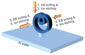
Regular Articles Vol. 12, No. 2, pp. 42–49, Feb. 2014. https://doi.org/10.53829/ntr201402ra1 Three-dimensional Nanofabrication in Si Using Electron Beam LithographyAbstractA new technique for fabricating three-dimensional (3D) nanostructures enables us to create various 3D nanodevices. The technique involves using electron beam (EB) writing from various directions on microstructures. New methods of resist coating on microstructures and etching parallel to the substrate surface make it possible to apply the 3D-EB writing to 3D nanofabrication in various materials, including Si and hard materials. This technique was used to create 3D Si nanostructures at high resolution and with a high fabrication speed and large arbitrariness in the types of 3D structures that can be created. The technique is therefore promising for creating 3D nanodevices in various nanotechnology fields such as nanomechanics and metamaterials. Keywords: EB writing, nanomechanical device, 3D nanostructure  1. IntroductionNanofabrication technologies such as those used in semiconductor manufacturing now have resolutions on the order of 10 nm. Because these technologies are generally based on layer-by-layer or planar techniques, we cannot use them to freely create real three-dimensional (3D) structures with such resolutions. However, we can create various items or machines using real 3D components on a macroscopic scale. An ability to freely create real 3D components and handle them on a microscopic scale will lead to the development of highly functional high-performance micro/nanoscale devices and equipment. In fact, various 3D micro/nanofabrication techniques based on concepts that differ from those in planar technologies have been reported for creating 3D nanodevices in various nanotechnology fields such as photonic crystals [1], [2], nanomechanical systems [3], [4], nanorobotics [5], [6], and metamaterials [7], [8]. However, each of the reported 3D techniques seems to have drawbacks such as poor resolution, time-consuming fabrication, or lack of arbitrariness in the applicable materials or the types of 3D structures that can be created. For example, techniques using ion beams [9], [10] or multiphoton absorption [8], [11] are limited to certain applicable materials, and the layer-by-layer [1] and thin-plate assembly [2] techniques are time-consuming or have low resolution in the vertical direction, depending on the number of layers. A versatile technique that could be used to create various 3D nanodevices would accelerate innovation in such nanotechnology fields. Such a technique should satisfy four major requirements: high resolution, high fabrication speed, applicability to various materials, and a large degree of freedom, that is, arbitrariness, in the types of structures that can be created. To realize such a technique, we have devised and improved 3D electron beam (EB) writing, which can delineate arbitrary patterns on microstructures [12]–[15]. By combining the writing with two newly devised methods—resist coating on vertical side faces of micrometer-order blocks on a substrate and ion etching parallel to the substrate surface—we have obtained a new 3D nanofabrication technique that achieves vastly superior total performance with respect to the four requirements mentioned above, compared to the conventional 3D techniques [16]. We describe here some demonstrations of the technique that confirmed its high level of performance and present some results for the two new methods. In addition, we propose a measure (quantitative index) of 3D nanofabrication speed. Application of this new technique to create 3D nanodevices in various nanotechnology fields will open up new avenues in 3D nanotechnology. 2. 3D fabrication process and experimentalOur 3D nanofabrication process is simply illustrated in Fig. 1. First, 2D EB writing and ion etching of a Si substrate are applied from the top to create microblocks on the substrate (steps 1 and 2). In these two steps, we use poly(methyl methacrylate) (PMMA) resist film about 500 nm thick and then apply EB writing at 100 kV (Vistec, VB-6UHR) on the film. Then, we use a lift-off technique with 300-nm-thick Ni film, and reactive ion etching (RIE) of about 4 μm using CF4/CHF3/O2 gases. Then, a resist film is spin-coated on the vertical side faces of the microblocks. PMMA resist film (70–100 nm thick) and an additional electroconductive polymer film (Showa Denko, Espacer®) are used. The method for coating these films on the side faces with good uniformity is described in subsection 4.1. Next, EB writing on the two opposite side faces of a microblock is performed (steps 3 and 4). The acceleration voltage, beam current, and beam diameter are 70 kV, about 50 pA, and about 7 nm. Details of this 3D-EB writing are described in literature [12]–[15], [17], [18]. Then, patterned masks are formed on the side faces. We use 30–60-nm-thick Ni films deposited with an EB evaporator; the unneeded films are then lifted off. Finally, RIE is carried out parallel to the substrate surface from the same side directions. This process etches through the microblocks and creates 3D nanostructures in single-crystal Si (steps 5 and 6). This RIE is performed in a 1.2-Pa vacuum with radio frequency power of 40 W using a RIE-10NR apparatus (SAMCO) and CF4/CHF3/O2 gases. The method of using RIE parallel to the substrate surface is described in detail in subsection 4.2. Baking before and after EB writing and photolithographic development after it were performed under conventional conditions. The substrate material used has little effect on the processing steps. Moreover, as also described in detail in subsection 4.1, coating the resist on the vertical side faces of a block is possible with various substrate materials as long as the resist solution wets the substrate. RIE can also be used with various materials, as it is often used in planar technology, although the mask material, gases, and other conditions may have to be carefully chosen depending on the materials. Therefore, in principle, materials do not impose limitations on this process.
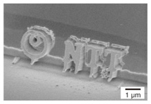
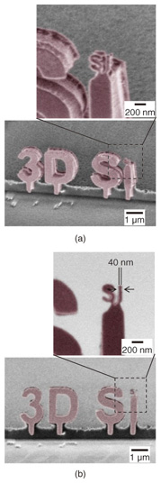
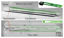
3. Demonstrations of techniqueScanning electron microscopy (SEM) images of 3D Si nanostructures that we created to demonstrate our technique are shown in Figs. 2, 3, and 4. It is clear from these images that our technique is effective for creating various 3D nanostructures in Si. The total EB writing times needed to create the structures in Figs. 2 and 3 were only about 1 and 2 s, respectively. Thus, the fabrication speed of our 3D technique is high. (A quantitative measure of fabrication speed is discussed in section 5.) The enlarged image in Fig. 3(b) shows that the minimum feature size is 40 nm, which means that our technique has a spatial resolution of 40 nm or less. The structure shown in Fig. 4 was designed and created as a nanomechanical cantilever. You can see that it is much more complicated than the nanostructures in Figs. 2 and 3. A cantilever about 40 μm long is attached to the base only through two nanobeams with sizes on the order of 100 nm, and there is a continuous change in thickness along the length of the cantilever. Note that if we had used conventional wet etching for a sacrificial layer, such fragile structures would have been broken by surface tension or by the flow of the etchant. The main difference in the fabrication process from that used for the simpler structures is that a complicated pattern shown as the inset of Fig. 4 (lower) is used in the first step of EB writing from the top instead of a simple rectangle. Even with this complicated pattern, all of the steps that follow can be performed in the same way, and such complicated structures can be created. Because we can, in principle, use arbitrary patterns in EB writing, this 3D technique allows us to create 3D nanostructures with great flexibility in the types of structures that can be created.
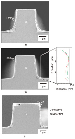
4. Key processing steps4.1 Coating resist on side facesCoating resist on the vertical side faces of microblocks with good uniformity is the first key to applying 3D-EB writing to various materials. Several methods for coating resist on non-flat surfaces with good uniformity have been reported. However, methods involving spraying resist solution [19], dipping a sample in solution [20], or keeping the sample in a mist of resist solution [21] are thought to be unsuitable for achieving good uniformity in the resist coating on the side faces of micrometer-order blocks. Evaporating resist with durability against high temperatures [22] is possible with certain resist materials, although they are severely limited. We recently discovered that high-speed spin-coating of a low-viscosity resist solution results in good uniformity in the thickness of the resist film coated on the side faces. When we spin-coat PMMA resist on micrometer-order blocks on a substrate using the conventional solution, we cannot obtain good uniformity on the side faces. As shown in the cross-sectional SEM image for typical PMMA (OEBR-1000, Tokyo Ohka Kogyo) (Fig. 5(a)), the resist becomes thicker at the lower (inner) edges and thinner around the upper (outer) ones. This is most likely because the surface tension of the solution reduces the surface area during coating. This solution uses 2-ethoxyethyl acetate as a solvent, which, in addition to the contribution from PMMA polymers, increases the viscosity. We found that when we coat our original solution (made by dissolving PMMA powder into a mixture of methyl ethyl ketone and hexane) at a spin speed as high as 6000 rpm, we can obtain good uniformity in the resist thickness on the vertical side faces (Fig. 5(b)). The viscosity of this solution is one to two orders of magnitude lower than the conventional solution. Therefore, since it flows faster during spin-coating, the force making it thinner at the inner edges, which is caused by its spinning-out, is thought to be larger than the force in the opposite direction due to its surface tension, and thus, uniform films on the side faces are obtained.
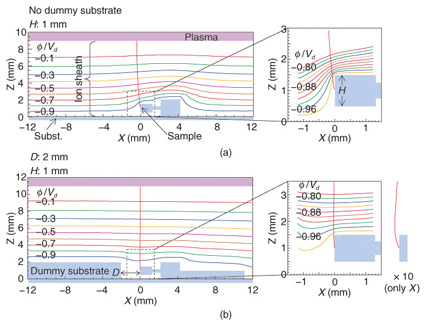
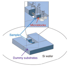
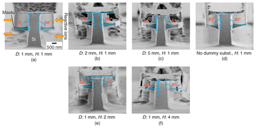
We propose a model to quantitatively understand this phenomenon as follows [17]. 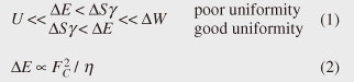 where U is the potential energy due to gravity, ΔS is the increase in surface area, γ is the surface tension (ΔSγ is the increase in surface energy due to the increase in surface area), ΔE is the decrease in energy due to spinning out of the solution, ΔW is the decrease in free energy due to wetting, FC is centrifugal force (per unit volume), and η is viscosity. When a solution flows along the side of a long microblock, it may be easier to consider Eqs. (1) and (2) per unit length along the side. Even if the block is as high as 1 mm, the increase in potential energy U for a solution to climb the block is much smaller than the other terms in inequality (1). Most resist solutions thoroughly wet substrates of various materials even during spin-coating at high speeds. This means that the decrease in free energy due to wetting, ΔW, is much larger than the other terms. The relationship between remaining terms ΔE and ΔSγ is thought to determine whether the uniformity of the resist on the side faces is good or poor. As expressed in Eq. (2), ΔE is proportional to the square of centrifugal force and inversely proportional to viscosity; that is, ΔE can be increased by increasing the spin speed and using a low-viscosity solution. Smaller surface tension, γ, is preferable for obtaining the lower relationship of inequality (1), but the difference is not large between the conventional solution and our solution. Actually, the estimated ΔE and ΔSγ under the conditions used for the resist coating in Figs. 5(a) and (b) are consistent with the relationship of inequality (1) [17]. This model indicates that we will be able to coat resist with good uniformity no matter what substrate material is used by preparing a resist solution with low viscosity and using a high spin speed so as to obtain the lower relationship of inequality (1). We also coated electroconductive polymer films on the side faces, as described in section 2. The default solvent for this is water, and it therefore has high surface tension and viscosity. We were not able to obtain good uniformity with the solution. By partly replacing the solvent and diluting it with ethanol, we were able to prepare a solution with low surface tension and viscosity. The resulting uniformity using the solution is good, as shown in Fig. 5(c). This supports our model in inequality (1) and suggests the wide applicability of our technique to various resist (and other film) materials in addition to various substrate materials. 4.2 Etching parallel to substrate surfaceThe other key step in our 3D nanofabrication is the method for etching microblocks from the side, that is, etching parallel to the substrate surface. We found that this becomes possible by keeping the sample height as low as 1 mm and by placing dummy substrates around the sample in the etching chamber. Many reports have been published on angled etching since the 1970s, but the reported etching angles range from approximately 40 to 75 degrees [23]–[25]. That is, no studies on etching parallel to the substrate surface have been reported. For example, setting a chip sample so it is vertically standing on edge in the chamber does not result in etching parallel to the substrate surface because the sample itself distorts the potential distribution around it, and thus, the ion trajectories bend near the sample, as shown in Fig. 6(a). We extended the method reported by Takamori et al. [24] by surrounding the small sample vertically aligned in the chamber with dummy substrates (Fig. 7). The key parameters in the configuration are the height of the sample, H, and the distance between the sample and dummy substrates, D. When both H and D are 1 mm, which were the minimum in our experiments, the maximum etching angle of 88 degrees is obtained. The cross-sectional SEM images in Fig. 8 show the etching angles with various H and D values.
We also performed theoretical calculations of etching angles and rates using the configuration shown in Fig. 7. The procedures consist of calculating 1) the spatial distribution of ion density in the ion sheath, 2) the potential distribution using the finite element method, and 3) the ion trajectories considering variations of the initial ion velocities. The calculation results agreed well with the experimental results derived from SEM images such as those in Fig. 8 [16]. Two of the calculation results are shown in Fig. 6 and clearly indicate that the ion trajectory without dummy substrates largely bends, resulting in a smaller etching angle (Fig. 6(a)), and that dummy substrates reduce the potential distortion, resulting in a straight ion trajectory and an etching angle very close to a right angle (Fig. 6(b)). The obtained maximum etching angle of 88 degrees is sufficient for our purpose, but a larger angle (closer to a right angle) should be obtainable by further reducing distance D between the sample and dummy substrates. 5. Index of 3D fabrication speedAs mentioned in section 1, several 3D fabrication techniques exist, and they all have certain advantages and disadvantages. This may make it a little difficult to fairly compare their fabrication speeds. A quantitative comparison is very useful, however, so we propose a measure (quantitative index) j of fabrication speed to make it possible to compare the 3D micro/nanofabrication speeds of various techniques: 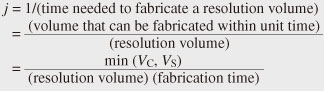 where (resolution volume) = (resolution)3 or, more strictly, (resolution along X) (resolution along Y) (resolution along Z) when resolution depends on direction, and VC and VS are the volume of the fabricated structure and the volume removed to make the structure, respectively. Resolution is defined by the minimum size of the feature/gap that is three-dimensionally fabricated. The fabrication speed of our technique is calculated from the structure shown in Fig. 3 to be about 80,000 resolution-volume units/s, where the total EB writing time (2 s) was used as the fabrication time. This speed should be in the top group among the 3D techniques described in section 1. Although the fabrication time does not include the time of other steps such as etching, it is appropriate because EB writing is the rate-determining step in the process. This concept––the use of the time of the rate-determining step as the fabrication time––is very common in planar fabrication technology because the time is directly related to throughput. For example, when a huge number of microstructures are etched at the same time in an etching chamber, the etching time per structure becomes negligible even if the total etching time is on the order of hours. On the contrary, an EB can write on only one microstructure at a time, so the EB writing becomes the rate-determining step. 6. ConclusionWe have devised a 3D nanofabrication technique that has high resolution (40 nm or better), high fabrication speed (80,000 resolution-volume units/s at least), wide applicability to various materials, and a large degree of freedom in the types of structures that can be created. The technique was realized by using our new methods of spin-coating resist with good uniformity on vertical side faces and etching parallel to the substrate surface. The technique is promising for developing 3D nanodevices in various fields such as nanomechanics and metamaterials. References
|
|||||||||||||||||||||||||||||||||||||||||||||||||||