 |
|||||||||||
|
|
|||||||||||
|
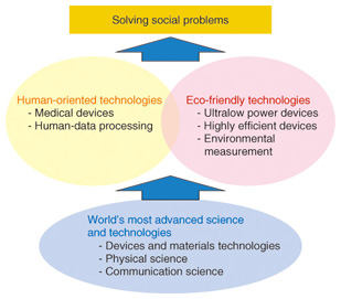
Feature Articles: Cutting-edge Device and Materials Technologies for Creating New Business Vol. 12, No. 4, pp. 22–26, Apr. 2014. https://doi.org/10.53829/ntr201404fa3 Innovative Services in Medicine, Healthcare, and Environment with Advanced Device and Materials TechnologiesAbstractDevice and materials technologies originally developed for the telecommunications industry can be applied to implement creative and competitive information and communications technology services. This article introduces some research and development activities we are pursuing for the creation of new business fields. Keywords: device, material, services 1. IntroductionScience and technology have progressed and matured greatly over the years, and many of the achievements in these areas have motivated researchers to create tools or systems for solving various existing social problems. These problems include, for example, many wrongdoings that have been exposed recently in the food and environment industries, whose operations should be subject to the highest standards because they are fundamental for safe and secure daily living. Another urgent issue is the increase in atmospheric carbon dioxide density caused by human activities, which is causing rises in temperature as well as unprecedented abnormal weather patterns around the world. There is also the aging society, which threatens the sustainability of our society because the ever increasing welfare and medical-care expenses for the elderly occupy a significant portion of the national budget. At the NTT laboratories, we are working to develop solutions to these social problems by employing our most advanced human- or environment-centric technologies. Our research and development (R&D) flow for solving the social problems is shown in Fig. 1. Our research fields include physical science, communications science, and device and materials engineering. Together, they provide a solid foundation on which to develop human-centric technologies such as medically oriented devices and data processing of human biomedical signals and environment-centric technologies such as highly efficient and ultralow-power-consumption devices.
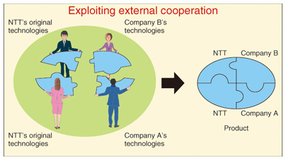
We are ready to license our intellectual property (IP) that has been created through our research. The effort to promote our IP to as many people as possible contributes not only to the telecommunications market but to other markets as well. 2. Exploiting external cooperationCompetitive devices and materials produced from research in the fields of smart living and life assistance can bring us many opportunities to create new business and expand our current business further. The expertise necessary for this kind of research, however, is quite diverse since it involves a deep technological hierarchy and broad application fields. This makes it much harder to complete the entire research process––from coming up with a concept to implementing an actual business framework––by ourselves. Exploiting outside technical resources is a key way to tackle this difficulty. We need to define what we can do by ourselves, spot technical elements that are lacking, and exploit outside resources effectively to compensate for the missing technical elements. Open innovation is a key practice, or attitude, for expediting the commercialization of products and services since it helps us use outside technologies whenever necessary without persisting in the use of our own technologies. A rule of thumb is to start external cooperation as early as possible to ensure there is sufficient time to establish a collaborative work relationship with outside organizations. This expedites the introduction of products and services with more value added to the market. This research attitude or practice that we are seeking is schematically shown in Fig. 2. We plan to continue this research practice strategically to create new business fields that expand our overall telecommunications business.
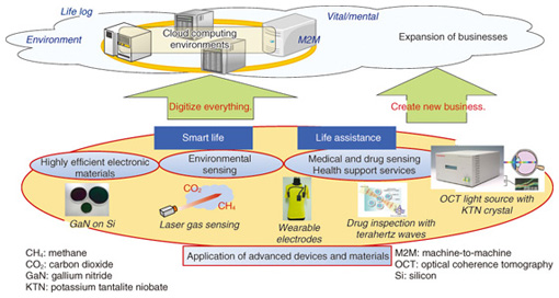
3. Sensing technologies and highly efficient electronic materialsSensing technologies are crucial for creating attractive services in the smart-life and life-assistance domains. Highly efficient electronic materials are vital for making energy-saving electronic appliances and thereby for supporting or sustaining our daily life with limited natural resources. We are creating new information and communications technology (ICT) services that employ novel sensing data acquired in the fields of medicine, healthcare, and the environment. This special issue highlights some of our sensing technologies and electronic materials, and provides detailed descriptions in individual articles. Those technologies and materials with links to their corresponding applications and ICT services are outlined in Fig. 3.
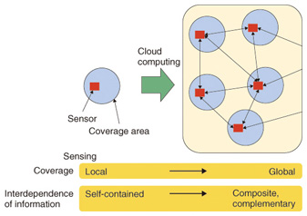
Future sensing technologies will be capable of integrating sensing data acquired from separate sources and as a result will be able to extract larger amounts of useful information than can be obtained by analyzing sensing data from a single source. Other physical phenomena that correlate with an original sensing source could add value to the analyzed information. From this viewpoint, cloud services will play a crucial role in creating innovative services in the fields of medicine, healthcare, and the environment. In these fields, various kinds of sensing data need to be easily exchanged, analyzed, and enhanced with additional values online in order for such services to become more feasible to general customers. Integrating sensing data with cloud services will help us advance related services, as illustrated in Fig. 4.
This special issue features five articles, each of which deals with promising technologies that can contribute to solving social problems in the fields of medicine, healthcare, and the environment. The first four articles describe sensing technologies, while the last one explains highly advanced electronic materials technologies. 4. Articles in this special issueThe first article, entitled “Electrocardiogram Monitoring Simply by Wearing a Shirt––For Medical, Healthcare, Sports, and Entertainment [1],” describes a sensing technology intended for measuring bioelectrical signals generated by the human body. NTT’s proprietary fabrication technique for bioelectrodes makes them flexible, durable, and biocompatible at the same time. These properties were once difficult to implement in conventional bioelectrodes. However, by wearing a compression shirt affixed with these biocompatible electrodes on the inside, the wearers can easily and continuously measure their own bioelectrical signals for long periods of time. The shirt has various applications, especially in the ICT domain, such as online advisory services in sports, healthcare, and medicine. The second article, entitled “200-kHz Swept Light Source Using a KTN Deflector and a High-speed Optical Coherence Tomography System [2],” explains a sensing technology for a medical diagnosis instrument. The medical diagnosis method called optical coherence tomography (OCT) is drawing a lot of attention these days because of its ability to quickly obtain cross-sectional images of biological tissue. NTT laboratories have successfully accelerated the rate at which a cross-sectional image can be captured by using a high-speed wavelength-swept light source fabricated with NTT’s proprietary KTN (potassium tantalite niobate) crystal. The acceleration can shorten the OCT procedure and thereby reduce the burden on patients. OCT cross-sectional images of biological tissue can be shared among hospitals over the Internet and can be analyzed with the help of cloud services to create new ICT services in medicine. The third article, entitled “Terahertz Spectroscopic Identification of Pharmaceutical Crystals: Cocrystals and Polymorphic Forms [3],” introduces a sensing technology intended for use in a drug inspection apparatus. In drug inspection, it is highly desirable to be able to observe the manner in which molecules bond to each other since such information can be used to determine a drug’s effectiveness. NTT’s proprietary terahertz-wave technologies enable us to observe molecular bonding, which has not been possible with conventional technologies. This inspection technique is attracting much attention for its use in clarifying how pharmaceutical crystals are dissolved and absorbed in the human body. The fourth article, entitled “Highly Sensitive Laser Based Trace-gas Sensor Technology and Its Application to Stable Isotope Ratio Analysis [4],” explains a sensing technology applicable to the analysis of food and atmospheric gasses. With NTT’s proprietary laser diode, we can analyze a tiny amount of an isotopic component with high sensitivity and cost effectiveness. The tiny amount of the isotopic component can be used as a signature for determining the origin of things, such as where or how they were produced. The signature can be obtained by investigating the ratio of the isotopic element contained in the targeted object. New ICT services such as preventing food fraud or monitoring sources of greenhouse gases could be implemented with this sensing technology in the near future. The fifth article, entitled “GaN-on-Si Technology for High-power Transistors [5],” describes a highly efficient electronic materials technology. NTT’s proprietary fabrication technique for growing GaN thin films on Si substrates makes it possible to produce more efficient and cost-effective electronic devices or more energy-efficient power devices than ever. This technology is attracting a great deal of interest because of its potential to reduce the environmental impact of our daily activities, particularly the impact of our use of electrical appliances. 5. Future prospectsThe technologies dealt with in this special issue vary in their development phase. Some are at an early stage where they are being tested to prove their applicability to their targeted fields. To refine such immature technologies for practical use, we need to simultaneously solve a lot of issues associated with reliability, safety, and cost. In this regard, cooperative work with other departments, laboratories, companies, and/or organizations is very effective and efficient since they can compensate for each other’s elements that are lacking. We have just started this cooperative research in some fields and are trying to expand it to other fields to expedite our competitive technologies for use in real products or services in the marketplace. References
|
|||||||||||

