|
|||||||||||||||
|
|
|||||||||||||||
|
Feature Articles: Cutting-edge Device and Materials Technologies for Creating New Business Vol. 12, No. 4, pp. 34–38, Apr. 2014. https://doi.org/10.53829/ntr201404fa5 200-kHz Swept Light Source Using a KTN Deflector and a High-speed Optical Coherence Tomography SystemAbstractOptical coherence tomography (OCT) using a swept light source can acquire cross-sectional images of tissue with micrometer resolution for biomedical applications. High-speed OCT imaging is important for achieving advanced volume rendering and for reducing the number of undesirable artifacts. Here, we report the development of a 200-kHz swept light source (SS) using a KTN (potassium tantalite niobate: KTa1-xNbxO3) deflector and a high-speed SS-OCT system, which we used to successfully obtain OCT images of a human finger. Keywords: optical coherence tomography, swept light source, KTa1-xNbxO3 (KTN)  1. IntroductionOptical coherence tomography (OCT) has attracted attention because of its potential use as a medical imaging technology [1]. OCT is an optical interferometry technique for acquiring cross-sectional images of tissue and other scattering materials with micrometer resolution. The resolution of OCT is higher than that of conventional imaging. Many studies related to two-dimensional (2D)-OCT imaging have been done. Three-dimensional (3D) OCT also promises to provide a more complete characterization of tissue structures on a par with those obtained with other medical imaging technologies [2]. However, 3D-OCT requires extremely high imaging speeds and data processing rates, in addition to the control of two scanning mirrors. OCT using a swept light source (SS-OCT) offers the potential for high-speed data acquisition. SS-OCT reduces the quality degradation of in-vivo OCT images of moving artifacts caused by movement of the body, and it also achieves rapid imaging with 3D-OCT [3]. SS-OCT detects wavelength-resolved interference fringes generated by a wavelength-scanning laser. A key component of the SS-OCT system is the light source. The desirable output characteristics of a swept light source include high power, a high repetition rate, and a broad sweep wavelength range. As the repetition rate of the light source is increased, the duration of the laser irradiation decreases and the quantity of data obtained within a fixed measurement duration increases. Thus far, such light sources have used mechanical actuators for wavelength scanning [4]. In contrast, we are developing a new light source that incorporates an electro-optic deflector that we plan to employ in a high-speed SS-OCT system. The deflector is based on a potassium tantalite niobate (KTa1-xNbxO3 (KTN)) single crystal. KTN has a very large electro-optic effect, which changes the refractive index by an applied voltage and bends the path of a light beam in a certain direction [5]. The deflection effect of the KTN is caused by a non- uniform electric field generated by injected carriers, and it exhibits a fast response and a fairly large light deflection angle [6]. The KTN deflector is useful for a fast repetition rate swept source. We have taken the advantages of KTN crystal into consideration in developing a new swept light source using the KTN deflector (Fig. 1). Furthermore, we are developing a high-speed SS-OCT system using the light source in order to achieve advanced image rendering.
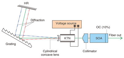
2. Swept light source with KTN deflectorThe setup of a swept light source equipped with a KTN deflector, which is based on a Littman-Metcalf cavity configuration, is shown in Fig. 2 [7]. The cavity consists of a 1.3-μm semiconductor optical amplifier (SOA) module, a collimator, a KTN deflector with electrodes, a cylindrical concave lens, a grating, and a high reflector (HR). The SOA module has a 10% reflector coupled to an optical fiber through an optical isolator on one side. The cavity length between the 10% reflector and the HR is about 60 mm. The KTN crystal is precharged by applying ± DC (direct current) voltage; then we scan the laser wavelength by applying a ±350-V sinusoidal voltage.
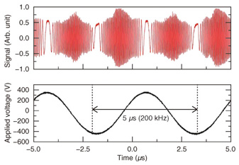
The light emitted from the SOA is collimated by the collimator, and it reaches the HR through the KTN deflector and the grating. The filter is constructed using the KTN deflector, the grating, and the HR. Light of a certain wavelength is selected according to the deflection angle of the KTN deflector, and it returns to the SOA. The 200-kHz voltage is applied to the KTN deflector, and the corresponding interference fringe signal is successfully obtained (Fig. 3). We also measured point-spread functions (PSFs), namely, the relative OCT signal intensity for a single-layer reflection at various optical delays between the sample and reference arms. The PSFs were obtained by fast Fourier transforming (FFT) the interference fringe signals. We observed a decrease in the interferometry fringe amplitude (or the peak height of its FFT) as we increased the optical delay. The measured coherence length in air was approximately 7 mm for a 200-kHz scan. This indicates that a depth range of several millimeters can be covered using this frequency swept light source.
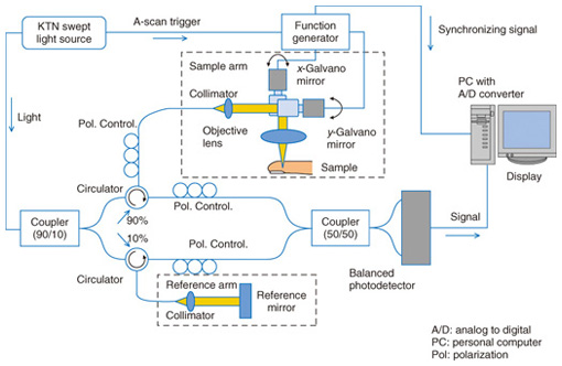
3. High-speed SS-OCT system using KTN swept light sourceThe high-speed OCT system is shown in Fig. 4. The setup consists of a swept light source with a KTN deflector, an optical fiber interferometer with a Mach-Zehnder configuration, galvano mirrors, and a computer for signal processing. The source outputs light at 20 mW around a center wavelength of 1.33 µm, with a wavelength scanning range of over 100 nm.
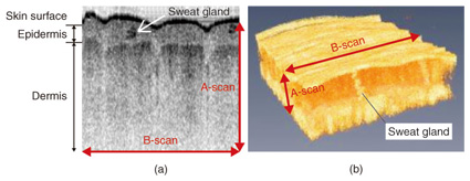
Light from the source is split by a 90/10 coupler into a sample arm and a reference arm. The light reflected from the reference mirror and from the sample is separated by respective optical circulators. Polarization controllers in both arms are used to adjust their polarization states. Light through the two arms interferes at a 50/50 coupler, the outputs of which are detected by a balanced photodetector. The light source also outputs an A-scan trigger in synchronization with a wavelength sweep. The A-scan triggers generate triggers of the galvano mirrors via a function generator. Interference fringe signals and synchronizing signals are recorded on a channel of a 10-bit data acquisition board at a sampling rate of 1-G sample/s. A depth profile, as a single A-scan, is obtained by the FFT of the interference fringe signal. In the 2D imaging, the x-galvano mirror of the sample arm is driven in synchronization with a B-scan trigger from the function generator. The beam scans a sample surface in the axial direction. All the signals for a single B-scan are detected and stored in the data acquisition board. A 2D image is constructed by mapping a transversal set of A-line scans. Furthermore, in the 3D imaging, in addition to the operation of the x-mirror, the y-galvano mirror of the sample arm is driven in synchronization with a C-scan trigger from the function generator. The beam performs an in-plane scan of the sample surface. A typical single C-scan consists of 200 sheets as B-scans, or 60,000 lines as A-scans. All of the data for a single C-scan are stored in the data acquisition board. A 3D image is constructed by post-processing the collected data. We acquired a 2D image of a human finger using the high-speed SS-OCT system. The image resolution was 200 × 200 pixels, and the image area was approximately 2 mm (horizontal) × 3 mm (depth), as shown in Fig. 5(a). The 2D image acquisition time was about 1.5 ms, which is several times faster than conventional SS-OCT systems. A 3D OCT image of the human finger with a 300 × 200 × 200 voxel resolution and a volume image area of 2 mm (horizontal) × 3 mm (vertical) × 3 mm (depth) is shown in Fig. 5(b). Here, the microstructures of the human skin including the epidermis, dermis, and a sweat gland are clearly visible as bright structures.
4. ConclusionWe have developed a high-speed swept light source using a KTN deflector for OCT. A 200-kHz scan rate was obtained with a 20-mW average output power at a wavelength scanning range exceeding 100 nm. The coherence length measured by using the relative signal decay from a different path delay was longer than 7 mm. We obtained 2D and 3D OCT images of a human finger using the OCT system equipped with the KTN swept light source. References
|
|||||||||||||||