|
|||||||||
|
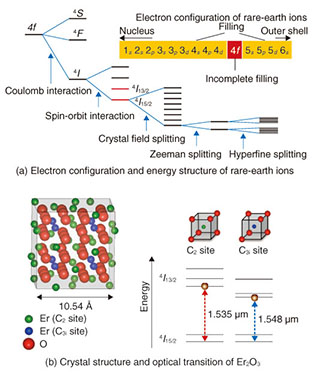
|
|||||||||
|
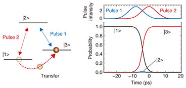
Feature Articles: Frontiers of Quantum Optics Research at NTT Basic Research Laboratories Vol. 12, No. 9, pp. 19–23, Sept. 2014. https://doi.org/10.53829/ntr201409fa4 Rare-earth Epitaxial Films as a Platform for Quantum Information ManipulationAbstractRare-earth ions in a solid form have discrete energy levels peculiar to the ionic species, and they are therefore expected to become an excellent platform material for quantum information manipulation. A promising candidate for this purpose is rare-earth epitaxial film such as erbium oxide (Er2O3) film grown on a silicon substrate. This article describes the high-quality crystal growth and excellent optical characteristics of Er2O3 epitaxial films for quantum information devices. Keywords: erbium oxide, population manipulation, energy transfer  1. IntroductionIn traditional telecommunication and data processing, information is transmitted as a classic light and voltage signal. However, we can expect the transmission quantity or speed with this approach to reach its limit in the near future. Today, information communication and processing techniques using photons and electrons based on the principles of quantum mechanics are being actively studied to overcome this limitation problem. The following methods are commonly used for quantum information communication and processing. Quantum information is transferred via optical polarization of a photon or electron spin state in a given material. A photon is used for the spatial transmission of information, and an electron is suitable for memory and information processing applications. The quantum information is exchanged between photons and electrons and manipulated by the photon-electron interaction. A critical issue with such a protocol is finding a way to improve the reliability of the exchanges and manipulation. Therefore, the selection of the material systems for the electron platform and the application of a suitable exchange and manipulation mechanism are especially important. Various materials and interaction mechanisms have already been proposed. Among these, we focus on stimulated Raman adiabatic passage (STIRAP), which uses three quantum levels as the principle of interaction (Fig. 1). In the STIRAP scheme with a lambda-type three-level system, the electron is initially in state |1>. After the irradiation of laser pulse 1, which leads to coupling between states |2> and |3>, the delayed laser pulse 2 (a photon with quantum information) causes excitation between states |1> and |2>, and the quantum information of this pulse is copied to an electron. Then the electron at state |1> transfers coherently to state |3> without passing state |2>. Here, a theoretical transfer efficiency of almost 100% is expected, and the quantum information of an electron can be maintained at state |3>, which has a long decay time [1]. Reverse transfer (from |3> to |1>) is also possible by using the opposite pulse sequence. Moreover, if another state (|4>) is prepared, a quantum bit as the information can be operated by employing STIRAP twice. That is, three (or four) ideal quantum levels that can interact with a photon enable the manipulation of all the quantum information [2].
2. Characteristics of rare-earth materialsWhat material system is suitable for quantum information manipulation based on STIRAP? Until now, this issue has been studied mainly using trapped atoms. While these are an ideal platform with deterministic, discrete, and non-perturbable quantum states, the equipment setup is complicated, and they are unsuitable for device applications. Semiconductor nanostructures such as quantum dots can be considered as other candidates that are advantageous for device application. However, it is difficult to prepare an ideal quantum level because of the quantum level energy fluctuation caused by the inhomogeneity of the structure and the energy broadening caused by a strong interaction with the crystalline environment. In contrast, rare-earth-doped solids are attractive as a robust material system for population manipulation in a solid, because they form deterministic and discrete quantum levels that do not depend on either host material or temperature. The intra-4f orbitals in rare-earth ions are weakly perturbed by the crystalline environment (Fig. 2(a)), and they form ideal quantum levels with only slight energy fluctuation. Erbium (Er) is a well-known rare-earth ion that is widely used in erbium-doped optical fiber amplifiers (EDFAs) in existing optical communications networks. The intra-4f orbital of an Er ion forms quantum levels that can interact with telecom-band photons (transition between 4I13/2 and 4I15/2 manifolds). Therefore, Er-based materials are very promising as a platform of STIRAP, and we are focusing in particular on epitaxial erbium oxide (Er2O3) thin films. [3] We have three reasons for this: 1. They have the highest concentration of Er ions per unit volume (2.7 × 1022 cm−3). 2. The intra-4f transition in Er ions is activated by coupling with oxide ions. 3. The lattice constant of Er2O3 matches that of Si(111). In conventional Er-doped crystal, concentration quenching is induced by defects when the Er ions are highly doped. On the contrary, in epitaxial Er2O3 thin films grown on a Si substrate, the generation of crystal defects is strongly suppressed without concentration quenching. Moreover, epitaxial Er2O3 on a Si substrate will enable on-chip integration with other functional devices such as light sources or detectors. The crystal structure of Er2O3 is shown in Fig. 2(b). The Er ions in this structure have two different sites with different symmetries, namely C2 and C3i. Because the crystal field differs at different sites, the energy levels also differ slightly between the C2 and C3i sites. In other words, the Er ion site that interacts with photons can be chosen by tuning the photon wavelength.
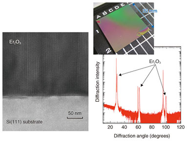
3. Fabrication of epitaxial Er2O3 on Si(111) substratesAn 85-nm-thick Er2O3 crystal was grown on a pure Si(111) surface by molecular beam epitaxy (MBE) at the optimum growth temperature and beam flux. As shown in Fig. 3, a cross-sectional transmission electron microscope (TEM) image obtained after growth proves that the Er2O3 was grown epitaxially on the Si(111) surface without any crystal defects. This is also proved by the X-ray diffraction pattern. Thus, we succeeded in growing epitaxial Er2O3 thin films with high crystalline quality on Si(111) substrates.
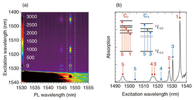
4. Population dynamics in discrete energy levelsTo characterize the quantum energy levels, we measured the photoluminescence (PL) spectrum of the grown Er2O3 samples at various excitation wavelengths [4] (Fig. 4). If the excitation wavelength corresponds to the Er2O3 energy level, the excitation photons are absorbed by electrons with the transition from the ground state of the 4I15/2 manifold to the excited state of the 4I13/2 manifold. After a certain lifetime, these excited electrons relax to the ground state with the photon emission. When the energy level does not agree with the excitation wavelength, since there is no photon absorption, the luminescence does not appear either. In the color plot in Fig. 4(a), when the figure is sliced in the vertical (horizontal) axis direction, it is equivalent to an absorption (emission) spectrum. The absorption spectrum detected at an emission wavelength of 1548 nm, which corresponds to the lowest energy transition of the C3i site (Fig. 4(b)), clearly reveals the formation of discrete and sharp energy levels. Since intense luminescence is also observed in the PL spectrum, concentration quenching is strongly suppressed by high quality epitaxial films without defects. The absorption peaks can be assigned to each energy level of the C2 and C3i sites by referring to theoretical analysis and experimental results for Er-doped materials. The absorption linewidth (full width at half maximum) is as narrow as 200 µeV. Since this is much narrower than the energy intervals of the 4I13/2 manifold, we can access each energy level optically.
Interestingly, these emissions from the C3i site appear even though the excitation energy resonates with the energy levels of the C2 site, which is separate from the C3i site. For instance, the peak with the red arrow labeled 1 in Fig. 4(b) indicates that both the strong absorption at the C2 site and the emission from the C3i site appear simultaneously. This means that energy is transferred unintentionally from the C2 site to the C3i site, since these sites are only about 3Å from each other, and this consequently induces a resonant energy transfer arising from a dipole-dipole interaction or wave function overlapping. We estimated this energy transfer time from the lifetime and the excitation power dependence of the PL spectra. As a result, we proved for the first time that the energy transfer is about 100 times faster (about 2 µs) than the relaxation between the excited and ground states. The energy transfer is inconvenient for a quantum information manipulation platform, because the electron carrying the quantum information escapes to irrelevant states, and the manipulation time is limited to the energy transfer time. However, in numerical simulations using the Er2O3 parameters, we obtained primitive results showing that the obtained energy transfer times are sufficiently long compared with the time required to complete the coherent population transfer operation in Er2O3 crystals (less than several tens of nanoseconds). Therefore, we believe that the energy transfer has no effect on the quantum information manipulation. 5. OutlookThis article described the growth and optical characteristics of epitaxial Er2O3 thin film, which is a promising material as a platform for quantum information manipulation. We recently succeeded in controlling the distance between Er ions without any energy transfer—that is, with the suppression of the Er-Er interaction. This also led to the further suppression of energy fluctuation in the quantum state and an increased electron transition decay time. In addition, we are investigating the coherence time and spin state of the Er intra-4f orbital. Our goal is to achieve quantum information manipulation with a solid material based on Er2O3 crystals that can operate with telecom-band photons. This work was a collaboration between NTT Basic Research Laboratories and Hokkaido University. References
|
|||||||||