|
|||||||
|
|
|||||||
|
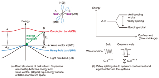
Feature Articles: Frontier Research on Low-dimensional Semiconductor Physics Vol. 13, No. 8, pp. 16–21, Aug. 2015. https://doi.org/10.53829/ntr201508fa4 Gate Tuning of Direct/Indirect Optical Transitions in SiliconAbstractSilicon is one of the most important semiconductor materials in microelectronics and is known as a typical indirect bandgap semiconductor. In these semiconductors, the minimal energy state in the conduction band and the maximal energy state in the valence band appear at different momenta. This makes it difficult to obtain efficient light emission. In this article, we present a means of electrically tuning the direct/indirect optical transitions using a specially prepared Si/SiO2 interface, where anomalously large valley splitting appears. This tunability is achieved by utilizing the close relationship between valley splitting and a direct optical transition in silicon and its proportional relationship with respect to a gate electric field. Keywords: quantum well, valley splitting, light-emitting devices  1. IntroductionThe continued miniaturization of silicon integrated circuits has considerably improved the performance of electronic information processors including computers and cell phones over the last decades. Similarly, optical communication technologies have improved significantly in both communication speed and capacity thanks to the development of compact and high-performance solid laser sources using compound semiconductors such as GaAs and InP. However, the recent remarkable increase in the amount of information requires further improvement in the performance of information processors. This is expected to involve the integration of optical components with electronic integrated circuits in order to meet the challenges presented by the limited bandwidth and power consumption of conventional metal lines used in processors and interconnects. Silicon photonics is a promising technology that enables both high speed and mass-information processing with low power consumption. By combining high-performance photonic building blocks such as waveguides, resonators, and modulators fabricated in silicon with complementary metal-oxide semiconductor (CMOS) technologies on the same chip, some companies have been able to release commercial products that achieve ultrahigh speed optical communications. However, the light source of such systems is made from exotic semiconductors (GaAs, InP) that are incompatible with silicon processing. This is because implementing a silicon-based light source is still a significant challenge due to its indirect bandgap nature, which is a fundamental property of bulk silicon. Therefore, laser components in the system are independently fabricated using an exotic semiconductor and then assembled in a silicon photonics system, which makes it difficult to reduce manufacturing costs. Having a silicon-based light source would drastically reduce costs and also increase performance thanks to the massive investment and existing knowledge of silicon CMOS technologies over the past decades, and therefore, the development of an efficient silicon-based light source is long-awaited. The study of silicon-based light sources goes back a long way. In the 1990s, many reports were published on methods to make silicon emit light using low-dimensional structures such as porous silicon and nanocrystals [1], where electrons are typically confined in a small space on the scale of a few nanometers. Most fundamental ideas on making silicon emit light are identical and involve confining an electron in a small space. This makes the electron’s wave function sharp in real space, and thus, a wave function is dispersed in momentum space, which in turn leads to a direct optical transition in silicon, which is known as a quasi-direct optical transition. In both porous silicon and nanocrystals, strong light emission can be seen even with the naked human eye due to the strong electron confinement. However, an ideal light source for silicon photonics requires certain properties: high stability in both wavelength and power, adjustability in emission wavelength, compatibility with the present silicon manufacturing process, and high efficiency in light emission. However, these silicon light sources have some problems in that they are physically unstable and difficult to inject current into due to their extremely small size and low-dimensional structure. It is also difficult to adjust the emission wavelength because of a lack of controllable parameters. We are working to solve these problems by applying electric tuning of direct/indirect optical transitions using a specially prepared Si/SiO2 interface, where anomalously large valley splitting appears. This electric tuning is a proof of concept demonstration that is based on the close relationship between valley splitting and a direct optical transition in silicon and its proportional relationship with respect to a gate electric field. Our silicon light-emitting devices are driven by current injection and fabricated using fully CMOS-compatible processes. They exhibit remarkably stable and reproducible optical characteristics thanks to the use of well-established silicon CMOS processes. 2. Electronic band and valley structures in siliconElectronic band structures in semiconductors are uniquely determined by the constituent elements of the lattice. Silicon has a diamond-type structure as well as an indirect bandgap, where the minimal energy states of the conduction band and the maximal energy state of the valence band are misaligned in momentum space. (Hereafter in this article, we regard a momentum as having the same meaning as wavenumber (k) because it has a linear relationship with the wavenumber.) Because the electron’s minimal energy state in the conduction band appears on [001] momentum axes near the X-point and there are three mutual axes, silicon has in total six energy-equivalent minima in its conduction band (Fig. 1(a)). These energy minima are called valleys because the states are first occupied by electrons with an increasing density, as if rain were pooling in valleys. The electrons in each valley can occupy the same space thanks to their different momenta even if they have the same energy (they are called degenerate). Since bulk crystal has a translational symmetry, the eigenstate of the electron in the system can be explained by a plane wave with a specific wavenumber (e−ik0·r), where the wavenumber k0 gives the minimal energy of the conduction band in the dispersion relation. This is known as the Bloch theorem. Suppose that spatial confinement normal to that of the [001] axes is introduced, and a quantum well (QW) is formed. Then the six-fold degenerate states split into two- and four-fold degenerate ones due to the anisotropy of electron effective mass, and accordingly, two valleys (labeled A and B in Fig. 1) lying along the confining axis become the ground states because they have heavier effective mass along the [001] axis. The eigenfunctions in the system are not a plane wave but a wave packet confined in the quantum well, as shown in Fig. 1(b). If we perform Fourier transform with respect to the wave packet, it becomes clear that the electrons are largely scattered in momentum space due to the confinement because it involves higher components of a Fourier coefficient. As the degree of confinement increases, further splitting (called valley splitting) occurs, where the two-fold degenerate valley states split, and thus, degeneracy is fully lifted. This splitting can happen when the Fourier coefficient that has a wave number that is nearly equal to the inverse value of the lattice constant (kz0~2π/a0) is finite. The resulting coupled states are called bonding and anti-bonding states, where the eigenfunctions are hybridized states of the +kz0 and −kz0 valley wave functions.
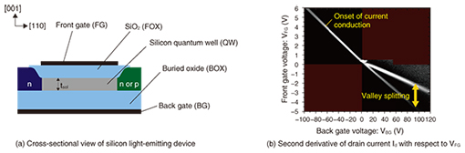
The valley splitting is tuned by the size of the QW, electric fields, or magnetic fields. In silicon metal-oxide semiconductor field effect transistors (MOSFETs), it can be tuned by gate electric fields. The typical size of valley splitting in general MOSFETs with gate oxides formed by the standard thermal oxidation process is at most several milli-electron volts, whereas NTT Basic Research Laboratories has reported large valley splitting up to several tens of milli-electron volts. The large valley splitting is observed in MOSFETs fabricated on a separation-by implantation-of-oxygen (SIMOX) wafer employing high-temperature thermal treatment [2], where SIMOX is one of the fabrication methods for a silicon on insulator (SOI), and a top silicon layer is separated by a buried oxide (BOX) formed by ion implantations of oxygen. The devices used in the present work are thin SOI-MOSFETs with a double-layer gate fabricated on a [001] SIMOX wafer employing high-temperature thermal treatment (Fig. 2). The front gate (FG) is constructed using polycrystalline silicon with a gate oxide (FOX) formed by conventional thermal oxidation. The substrate is used as a back gate (BG). Both n- and p-type contacts are formed to inject the carriers into the QW sandwiched between the FOX and the BOX. Both FG and BG voltages (VFG, VBG) are applied in order to control the distribution of both electrons and holes in the QW.
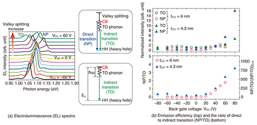
When positive VFG and negative VBG are applied, electrons are squeezed into the FOX interface. Since the size of valley splitting is quite small at the interface, only the onset of current conduction can be detected as a white line in Fig. 2(b). In contrast, when the polarities of both gates are mutually replaced, electrons are squeezed into the BOX interface, and the white line gradually splits. This splitting is just the valley splitting that we discuss in the following sections. Although the physical origin of the large valley splitting remains unclear and is still under debate, the notable points here are that the electrons’ wave functions are strongly dispersed in momentum space when the electrons are distributed at the BOX interface, and the size of valley splitting is tunable by gate electric fields. 3. Relationship between valley splitting and dipole transitionsNext, we examine an application of large valley splitting to light emission for indirect semiconductors. Light emission is known to occur when an electron relaxes from an initial higher energy state to a final lower one and loses its energy as a photon. Since photons do not carry a significant momentum, and both the energy and momentum are preserved in any physical process, the momentum of an electron in the initial higher state is preserved in pure direct optical transition. In contrast, in bulk silicon, the minimal energy states of the conduction and valence bands have different respective momenta. This means that such a transition rarely occurs in bulk silicon. Despite this, weak light emission is observed in bulk silicon thanks to the aid of phonons. This process, which is called an indirect optical transition, can be completed only when an electron absorbs or emits a phonon with the momentum kz0 and also emits a photon with the energy corresponding to the value of the phonon energy (ћω) subtracted from the bandgap of silicon (Eg). Although this process occurs more frequently than the pure direct optical transition in indirect semiconductors, another non-radiative process such as Auger or free-carrier absorption quickly recombines an electron, and therefore, the photon emission efficiency is quite low in indirect semiconductors. This is why silicon is inappropriate for light-emitting devices. With finite valley splitting, the wave function of electrons in the QW is composed of a broad range of components for a Fourier coefficient, as discussed in the previous section. If the amplitude of 2kz0 components does not have a zero value, then a direct optical transition can occur. This is because the variation of the confining potential formed by the gate electric field is much gentler than that at a steep Si/SiO2 interface, so the wave function confined by the gate electric field has a smooth profile. The profile of such a smooth wave function gently varies as the gate electric field increases, where the amplitude of the kz0 component follows that of 2kz0. Therefore, it is expected that large valley splitting will lead to significant direct optical transitions. 4. Electric tuning of direct/indirect optical transitionsWe then examined light emission using finite valley splitting. In this experiment, light emission was achieved by electroluminescence (EL), where both carriers were electrons and holes and were injected into the channel. We used n- and p-type contacts as a respective source and drain. We applied forward bias and injected carriers into the QW; then we tuned both gate biases VFG and VBG so as to control the distribution of the electron and hole wave functions. EL spectra as a function of VBG are shown in Fig. 3(a), where the sizes of valley splitting are adjusted by tuning both gates (FG and BG). When we applied positive VFG and negative VBG, a transverse optical (TO) phonon-mediated indirect optical transition dominated the spectra. This transition is the main radiative recombination process in bulk silicon. In contrast, when the polarities of both gates were mutually replaced, a higher energy peak gradually developed with an increasing VBG. The energy separation between TO and the higher energy peak are approximately 59 meV. The energy separation agrees with the energy of the TO phonon with a momentum at valley minimum (kz0). When we take into consideration these peak energies with the energy separation, the higher energy peak is assigned as a non-phonon (NP) direct optical transition, where the electron in the conduction band minima directly recombines with the hole in the valence band without aid of the phonon. The intensities of the NP peak increase with an increasing |VBG| and they greatly increase for a positive VBG. Eventually, the intensity of the NP peak becomes larger than that of the TO phonon-mediated indirect optical transition. The efficiency of light emission is plotted in Fig. 3(b) taking into account the current flowing in the QW that becomes small as valley splitting increases. We assumed a condition close to the bulk silicon by applying zero gate voltages to both the FG and BG, and using a thicker QW. We define this as the bulk condition. The efficiency of the NP direct optical transition is 16 times better than that of the TO phonon-mediated indirect optical transition in the bulk condition. Weak NP direct optical transitions are known to occur even in bulk silicon thanks to an unintentionally doped slight amount of impurities that bind electrons around them and disperse the electrons’ wave function. We have found that the optimal efficiency of the NP optical transition was 800 times greater than the NP direct optical transition in the bulk condition [3]. Furthermore, the ratio of NP/TO is tuned by the gate electric field. This is the world’s first demonstration of electric tuning of direct/indirect optical transition in silicon by controlling the size of valley splitting at the Si/SiO2 interface.
5. ConclusionWe reported electric tuning of direct optical transitions up to 800 times greater than that in bulk silicon. However, the efficiency of such a direct optical transition is much weaker than that in GaAs or InP, and of course, this is not sufficient for implementing silicon light-emitting devices. Therefore, we will examine hybrid approaches that combine elements such as impurities and photonic crystals in order to improve the light emission efficiency. References
|
|||||||