|
|||||||||||||||||||||||||||||||||||||||||
|
|
|||||||||||||||||||||||||||||||||||||||||
|
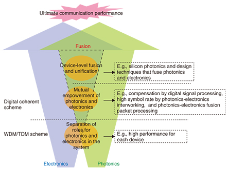
Feature Articles: Photonics-electronics Convergence Hardware Technology for Maximizing Network Performance Vol. 14, No. 1, pp. 12–18, Jan. 2016. https://doi.org/10.53829/ntr201601fa1 R&D Trends in Convergence of Photonic and Electronic Hardware for Network InnovationAbstractNetwork traffic will continue to increase exponentially as we get closer to deploying fifth generation mobile networks, and as the Internet of Things and big data services expand through 2020 and beyond. In these Feature Articles, we look at trends in the research and development of advanced hardware technology designed to achieve substantial increases in the capacity of communication networks with much lower capital and operating expenditures in the next 5 to 10 years. We focus in particular on technology based on new concepts and principles that involve the convergence of photonics and electronics. Keywords: photonics-electronics convergence, networks, hardware  1. IntroductionThe rapid spread of smartphones around the world is increasing network traffic exponentially. In the next five years, the amount of traffic is expected to increase by a factor of 10 [1]. Development of the fifth-generation mobile network (5G) expected to be launched beginning in 2020 is proceeding rapidly. Specifically, efforts are underway to achieve substantially higher capacity per square kilometer—by a factor of 1000 or more—compared to the present LTE (Long-Term Evolution) system [2]. The movement toward the Internet of Things is also accelerating. One recent key term is Industry 4.0, which refers to improving the efficiency of production and services by implementing a cycle of various types of sensing, signal and knowledge processing, and optimization control. Ultimately, the astronomical amount of sensor data on human activity, objects, and the environment will be distributed via the network, and such data will be a source for big data services driven by machine learning. The virtualization of computations and networks continues to progress, and this means that huge amounts of network traffic will be processed in a cloud environment by enormous datacenters. The Internet protocol traffic of the world’s datacenters is expected to triple over the five years from 2013 to 2018, and three-fourths of that is expected to consist of traffic within the datacenters. 2. Convergence of photonic and electronic technology: device technology for network innovationA photonic network is a huge system that combines photonic and electronic technology. It comprises optical transceivers, node equipment (electrical or optical switches or routers), and servers. This equipment is implemented by a combination of electronic and optical hardware. The concept of converging photonic and electronic communication hardware is illustrated in Fig. 1. Photonic network communication has evolved through innovation of transmission technology such as time division multiplexing (TDM) and wavelength division multiplexing (WDM), and through innovation of optical and electrical devices. Digital coherent technology [3] is a revolutionary idea that is enabling communication over 100 Gbit/s per wavelength and over distances of thousands of kilometers. Digital signal processing LSIs (large-scale integrated circuits) constructed using state-of-the-art semiconductor process technology suppress various types of fluctuation and noise in the communication channel, and they have achieved a level of performance that has never been achieved before by individual improvements in optical and electrical devices alone. In the future, the synergistic effect and mutual compensation obtained by combining photonic and electronic technology including digital signal processing may hold the key to even further network innovation.
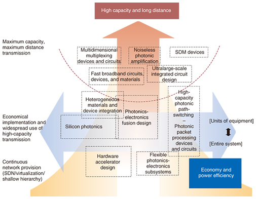
One direction for progress is device-level convergence. For example, silicon photonics technology is expected to produce a paradigm shift in telecom hardware by increasing its functionality and reducing its size, cost, and power consumption through a high level of integration of optical and electrical devices. These Feature Articles introduce some of the research and development (R&D) on hardware being conducted at NTT Device Technology Laboratories to achieve network innovation. The first part focuses on cutting-edge technologies for converging photonic and electronic devices, which are aimed at achieving the ultimate in network capacity. The second part describes technology for achieving a radical decrease in cost and power consumption as well as higher capacity. This technology is essential to sustain the progress achieved in networks requiring a much higher level of economy and energy efficiency such as datacenters. We also introduce research on hardware technology to achieve network virtualization in the software-defined networking (SDN) era for reducing capital expenditure (CAPEX) and operating expenditure (OPEX). A mapping of the technology for these two directions is shown in Fig. 2.
3. Hardware technology for ultimate high capacity: challenge to achieve ultimate high symbol rateTo increase the capacity of photonic networks, technology must expand along three axes: the number of multilevels, the number of subcarriers*1, and the symbol rate*2. For example, recent digital coherent optical communication systems have achieved a transmission rate on the level of 400 Gbit/s by using 16QAM (16-level quadrature amplitude modulation)*3 and two-subcarrier multiplexing [4]. Of the hardware research being done to expand the three dimensions mentioned above, the research aimed at increasing the symbol rate can increase the capacity with the same number of subcarriers and multilevels, so it is advantageous in that it simplifies ultrahigh capacity transceivers. The symbol rate for the current 100-Gbit/s digital coherent systems is 32 Gbaud, but research is ongoing to achieve even higher speeds. The article “High-speed Electronic and Optical Device Technologies for Ultralarge-capacity Optical Transmission” [5] in this issue describes an effort to greatly increase the symbol rate through conversion of ultrahigh speed indium phosphide (InP) integrated circuits and OTDM (optical time-division multiplexing). 3.1 SDM technology for drastic increase in capacityExtensive R&D is being done on space division multiplexing (SDM), which targets a drastic increase in capacity that exceeds the physical limits of conventional single-mode optical fiber [6]. SDM can increase the transmission capacity by a factor of several tens by making maximum use of the spatial degrees of freedom in an optical fiber. This is done by using multicore fiber, which has many cores in a single fiber, or by using multiple waveguide modes within a single core for multimode transmission. The ongoing research toward implementation of SDM includes work on erbium-doped fiber amplifiers (EDFAs) as optical amplifiers for long-distance multicore and/or multimode transmission, and connection devices that are required for branching and converging with single-mode fibers, in addition to many-core optical fiber. It also includes signal processing methods for compensating interference between modes within a core [7]. 3.2 Challenging the Shannon limit: a noiseless optical amplifierAccording to Shannon’s theory, the capacity of a communication channel is expressed by the following equation,
To cope with this situation, NTT is working on research to improve the SNR by applying phase sensitive amplifier (PSA) technology. A PSA uses parametric amplification by a periodically polled lithium niobate (PPLN)*4 device, which has a highly nonlinear optical effect. With the PSA, amplification with no degradation of the SNR is theoretically possible, and a doubling of the transmission distance can be expected in theory. This technology is explained in the article “Advances in Phase Sensitive Amplifiers Based on PPLN Waveguides for Optical Communication” [8] in this issue.
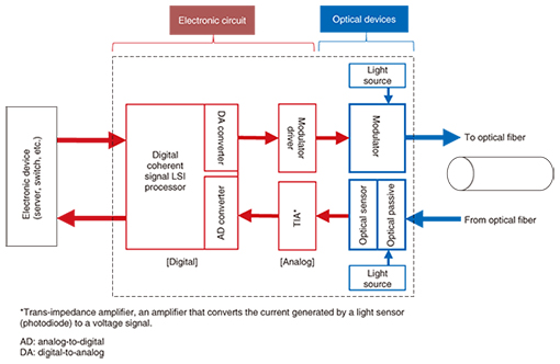
4. Hardware technology for economical network innovation (towards smaller and more energy-efficient hardware)4.1 Device-level photonics-electronics convergence: silicon photonicsSilicon photonics is technology for integrating electronic circuits and optical circuits/components on a silicon chip. One of its major advantages is that it makes it possible to achieve ultra-compact optical circuits. The dimension of waveguide fabrication and radius of curvature are a few orders of magnitude smaller than for the glass (SiO2) generally used in optical circuits. This can reduce the optical circuit size from centimeter- to millimeter-order. Furthermore, integration with large-scale complementary metal-oxide semiconductor (CMOS) digital circuits with high functionality will lead to an ideal photonics-electronics convergence system-on-a-chip with a smaller, less expensive form. NTT has been leading the silicon photonics research field and has achieved cutting-edge results for a Si (silicon)-based multiparallel integrated WDM receiver and other advanced devices [9]. The article “Lateral Current-injection Membrane Lasers Fabricated on a Silicon Substrate” [10] explains the cutting-edge optical source integration technology used to integrate a low power consumption InP side-injected thin-film laser on a silicon substrate. The greatest barrier to widespread use of silicon photonics is that the light-emitting capability of silicon itself is very low. We are working to overcome that problem by achieving true silicon photonics. 4.2 Device-level photonics-electronics convergence: digital mock-upComplexity in the convergence design is a serious obstacle to radically reducing the hardware cost. The optical transceiver shown in Fig. 3 comprises both optical and electronic devices. In the conventional design procedure, performance prediction and simple modeling are done only for the optical circuit at first, and the results are input to an electronic circuit simulator to estimate the overall performance. However, performance prediction for a total system is difficult, so repeated test device fabrications are necessary. That process increases the design and manufacturing cost. The article “Photonics-electronics Convergence Design for Digital Mock-up” [11] in this issue describes technology for implementing digital mock-ups that can estimate the convergence hardware performance with high accuracy and without making a series of test devices. In the future, the boundary between photonic and electronic circuits will become blurred in a good sense, both physically and functionally in the silicon photonics era. This technology can be expected to enable design that extracts maximum performance with less cost for photonics-electronics convergence devices.
5. Ultrafast optical switching device technology for extending the scalability of datacentersLarge-scale datacenters are used to support cloud computing and big data processing. These datacenters house hundreds of thousands of servers that are connected hierarchically by a large number of network nodes (L2/L3 switches and routers). However, the high latency and huge power consumption of the large numbers and layers of node units are serious problems. Current routers and switches are electronic equipment that consists of integrated circuits. As we approach the limit of Moore’s law*5, it is becoming difficult to solve these problems only by increasing the speed and reducing the power consumption of circuits. The article “High-speed Optical Packet Switching for Photonic Datacenter Networks” [12] describes the innovative research on a photonic implementation of packet-by-packet switching, which has so far been done by conventional electronic routers and switches. Low-latency optical packet switching without opto-electrical conversion is being developed as a solution to these problems. NTT has been leading the world with its cutting-edge research on optical packet switching technology, and has proposed a hybrid opto-electric packet router that combines an ultrafast (nanosecond-order) optical switching device and an electronic buffer (integrated circuit memory).
6. Hardware technology for advancing SDN and virtualizationStudies on network virtualization are moving forward with the objective of reducing network CAPEX and OPEX. In network function virtualization (NFV), network functions that have previously been implemented as dedicated hardware are implemented in software that runs on servers. The expected advantages of virtualization include flexible allocation of resources and rapid service provision and modification, as well as reduction of hardware costs [13]. General-purpose servers use the most advanced microprocessors, but the future rate of improvement in semiconductor performance is expected to lag behind the increase in network capacity. As we enter the future terabit era, it is expected to be difficult to obtain speed and power efficiency through the flexibility of NFV. The article “Hardware/Software Co-design Technology for Network Virtualization” [14] in this issue describes hardware accelerator technology as one direction for research on hardware in the era of SDN and virtualization. In that approach, functions that are bottlenecks in improving performance speed are carefully selected and implemented using a more hard-wired method with the objective of raising the cost performance of NFV implemented on general-purpose servers. The acceleration effect was verified by using the Lagopus software switch platform developed by NTT Network Innovation Laboratories [15]. References
|
|||||||||||||||||||||||||||||||||||||||||