|
|||||||||||||||||||||||||
|
|
|||||||||||||||||||||||||
|
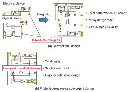
Feature Articles: Photonics-electronics Convergence Hardware Technology for Maximizing Network Performance Vol. 14, No. 1, pp. 38–44, Jan. 2016. https://doi.org/10.53829/ntr201601fa5 Photonics-electronics Convergence Design for Digital Mock-upAbstractWe developed a design technique for an electronic and photonic integrated circuit that involves using an equivalent circuit of optical devices in an electrical circuit simulator. Key features are the use of structural and physical parameters as calculation parameters in the equivalent circuit to provide a practical device design and the use of an intermediate frequency to model the wavelength dependence of optical devices in an electrical circuit simulator. By combining these techniques, we simulated the bit error rates and eye diagrams of a device that integrates an optical and electrical circuit. This technique turns an electrical circuit simulator into a photonics-electronics convergence simulator. Keywords: photonics-electronics convergence, digital mock-up, equivalent circuit  1. Introduction1.1 Photonics-electronics convergenceTelecommunications network systems are now facing an explosive traffic increase, with a growth rate of 30% per year [1]. At this growth rate, the power consumption and capital/operating expenditures for network systems will increase by ten times or more. One of the breakthrough technologies for dealing with this information explosion is photonics-electronics convergence. Photonics-electronics convergence devices, which comprise both optical and electrical components, can achieve performance that far exceeds that of discrete devices. Moreover, their high integration density and low power consumption make them promising devices for reducing network costs [2–4]. Photonics-electronics convergence devices are more than just combinations of electrical and optical circuits. They involve high-density integration that provides organized functions and high performance. Thus, a photonics-electronics convergence device must comprise integrated circuits. However, dense and functional integration leads to complex designs and high fabrication costs. To reduce fabrication costs, we need to estimate the performance of an integrated circuit before it is fabricated. For this purpose, NTT Device Technology Laboratories has focused on developing a technique to design photonics-electronics convergence. Conventionally, optical and electrical devices are designed individually to obtain the optimal performance of an integrated device, as shown in Fig. 1(a). However, as mentioned above, the actual performance of integrated devices does not correspond to the performance of the combined discrete optical and electrical devices. For this reason, optical and electrical devices should be designed in a cooperative manner by converting and sharing data to maximize the total performance of integrated devices. However, the potentially very large computational cost of data conversion and sharing could become a bottleneck in the overall design. Furthermore, in the data sharing process, each design tool can only share limited information such as output waveforms, scattering parameters, and DC (direct current) and AC (alternating current) responses. This limitation impedes the overall design, which increases the time and cost. In addition, many software licenses are required, which increases the capital cost for the design. 1.2 New design techniqueNTT Device Technology Laboratories has devised a photonics-electronics convergence design technique to solve these cost problems. The design involves the use of a unified platform to design both optical and electrical devices and simulate overall performance (Fig. 1(b)). This approach eliminates the need for data conversion/sharing and software licenses and guarantees that information about devices is not lost. In other words, it reduces the computational and capital costs, as well as the required time. This design technique, referred to as a digital mock-up, uses precise design and simulation models that reduce the number of trial fabrications to zero. As a final objective of the photonics-electronics convergence design, we aimed to construct a digital mock-up for a photonics-electronics convergence device.
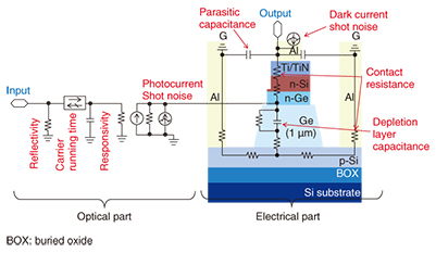
The first step in providing the digital mock-up was to use an electrical circuit simulator as a unified design platform. This eliminates the need for an optical device simulator and enables us to design everything in one simulator. This unified platform is familiar to people in the electrical circuit field and is compatible with electronic design automation. Since a photonics-electronics convergence device has many more electrical elements than optical ones, the use of an electrical circuit simulator as a unified design platform is efficient from the viewpoint of computational cost. There are two important points for modeling optical devices in an electrical circuit simulator. One is that the models should be able to handle the physical and structural parameters for designing them. The other is that the electrical circuit simulator must handle characteristics that cannot be used as calculation parameters in a conventional electrical circuit simulator but that are necessary for optical circuits. The necessary parameters for simulating optical devices are wavelength, polarization, and waveguide mode, but an electrical circuit simulator cannot handle them. In this study, we used an equivalent circuit of an optical device in an electrical circuit simulator for photonics-electronics convergence design. Other design techniques have used equivalent circuits of optical devices in an electrical circuit simulator [5–7]. However, a conventional equivalent circuit uses several lumped elements to express only the frequency response of optical devices. It cannot use device structures or physical parameters as calculation parameters. Thus, when an optical device is redesigned, the equivalent circuit has to be modeled again. To design an optical device in an electrical circuit simulator, the equivalent circuit should consist of lumped elements that have a one-to-one correspondence with the structural components and physical parameters of an actual device. This allows us to carry out structural and material redesigns of optical devices in an electrical circuit simulator by changing the parameters of the lumped elements. 2. Design of optical equivalent circuits2.1 Model for designing optical devices in an electrical circuit simulatorIn this study, we used a germanium photodiode (Ge-PD) for the optical device, as shown in Fig. 2. We used lumped elements in our equivalent circuit and divided it into electrical and optical parts. The electrical part consists of the contact resistances, the capacitance and resistance of the depletion layer, shot noise due to dark current, and the parasitic capacitance between electrodes. These parameters of the lumped elements are independent of each other and have a one-to-one correspondence with the structural components of an actual Ge-PD.
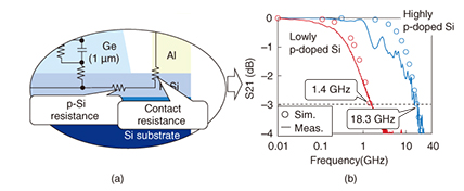
The optical part of the equivalent circuit includes the optical parameters of the Ge-PD, which are responsivity, carrier running time, shot noise due to photocurrent, and reflectivity. The shot noise due to photocurrent is a function of the input optical power. The capacitance for carrier running time models the frequency dependence due to carrier drift in a Ge layer as a simple low-pass filter. The lumped elements reflect the structure and physical parameters of the Ge-PD, and the circuit parameters depend on the dimensions and material parameters. Thus, we can achieve a simple structural design of an optical device by using this equivalent circuit. We fabricated, characterized, and simulated Ge-PDs with the same structure as in Fig. 2 to confirm the feasibility of our equivalent circuit. The detailed structure, fabrication process, and performance of the Ge-PD are described in our previous reports [8–10]. The measured and simulated S21 parameters for Ge-PDs with a heavily or lightly p-doped Si layer are plotted in Fig. 3(b). The doping concentration of Si determines the contact and p-doped Si resistance as shown in Fig. 3(a), which mainly determines the total resistance of the Ge-PD. In the measurement, the Ge-PD with the lightly doped Si layer shows a lower 3-dB cutoff frequency than that with the heavily doped one, as shown in Fig. 3(b). In the simulation, we changed the parameters of the two resistances, whose values were estimated from a test element group. As shown in Fig. 3, the agreement between the simulated and measured frequency responses of the Ge-PD is very good, which means that we can design optical devices by changing the parameters of the lumped elements.
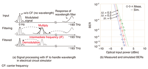
2.2 Model for handling unique parameters of optical devices in an electrical circuit simulatorIn this study, we used as an example the wavelength characteristic of optical devices. The method for handling wavelength in the electrical circuit simulator, in this case for a wavelength filter, is shown in Fig. 4. Details of the wavelength filter are described in our previous paper [9]. A modulated optical signal can be considered to be a modulation signal with a very high carrier frequency. In the conventional method, the carrier frequency, which is about 193 THz, is ignored because it is too high for an electrical circuit simulator to handle. In this study, we down-converted the carrier frequency and the frequency response to an intermediate frequency (IF). We use the IF as a pseudo-carrier frequency to indicate the wavelength dependence in an optical device. The signal processing with an IF to handle wavelength in an electrical circuit simulator is shown in Fig. 4(a). An input signal is multiplied by the IF, and the center frequency of the wavelength filter is down-converted to it. Optical signal processing such as filtering and phase modulation is performed around the IF. Finally, the carrier frequency is removed, and the envelope signal is extracted.
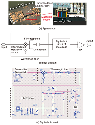
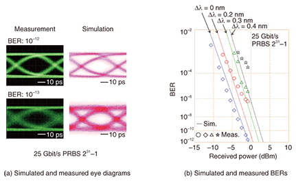
The measured and calculated bit error rates (BERs) of a signal after it has passed through a wavelength filter are shown in Fig. 4(b). Here, Δλ is defined as the difference between the IF and the center frequency of the ring resonator response. The pseudo-random bit sequence (PRBS) transmission word length and data rate were 231–1 and 12 Gbit/s. As Δλ increases, the BERs shift to the high input power side because the input signal should compensate for a power penalty due to the wavelength filter. In the calculation, the BERs agree well, with the difference being at most 1 dB. The power penalty due to the wavelength shift is properly depicted. We concluded from the simulation results that we have managed to use the IF to model the wavelength dependence in an electrical circuit simulator. 3. Measurement and simulation results for optical receiver with integrated electrical circuitWe fabricated an actual silicon photonic optical receiver with our in-house transimpedance amplifier (TIA) as a test device for photonics-electronics convergence simulation, as shown in Fig. 5. A block diagram of the optical receiver is illustrated in Fig. 5(b). It contains a wavelength filter, a Ge-PD, and the TIA. As shown in Fig. 5(a), these devices are integrated densely on one chip. Details of the optical receiver are described in our previous papers [11, 12]. An equivalent circuit of the optical receiver is shown in Fig. 5(c). We used a simplified TIA model to reduce the computational cost. The parameters of this simplified TIA block are the frequency response, input referred noise, and transimpedance. These parameters are determined from the discrete TIA chip. The simulated and measured eye diagrams and BERs of the optical receiver for Δλ = 0, 0.2, 0.3, and 0.4 nm are given in Fig. 6. The PRBS word length and bit rate were 231−1 and 25 Gbit/s. The IF was set at 200 GHz. The measured and simulated BERs agree well, with an error less than 3 dB, and the simulations properly depict the power penalty due to a wavelength shift. Thus, we can conclude that we were able to successfully simulate a photonics-electronics convergence device. In other words, we can design photonics-electronics convergence devices using an electrical circuit simulator as a unified design platform.
4. SummaryWe developed a design technique for photonics-electronics convergence that uses equivalent circuits of optical devices in an electrical circuit simulator. The technique uses the physical parameters and dimensions of optical devices as calculation parameters. This allows us to design optical devices in an electrical circuit simulator. We also use an intermediate frequency to model the wavelength dependence of an optical device. We combined these techniques to simulate the BER and eye patterns of a Si photonics optical-electrical integrated receiver. The simulated and measured BERs and eye diagrams showed good agreement, and the power penalty due to the wavelength shift was properly depicted. This technique uses only the ordinary functions of the electrical circuit simulator. It does not require any other simulator platform. Thus, the electrical circuit simulator becomes a photonics-electronics convergence simulator by virtue of the equivalent circuit of optical devices. This is the first step to establishing a photonics-electronics convergence design for digital mock-up. References
|
|||||||||||||||||||||||||