|
|||||||||||||||||||
|
|
|||||||||||||||||||
|
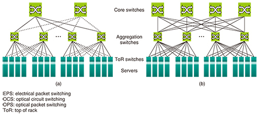
Feature Articles: Photonics-electronics Convergence Hardware Technology for Maximizing Network Performance Vol. 14, No. 1, pp. 45–51, Jan. 2016. https://doi.org/10.53829/ntr201601fa6 High-speed Optical Packet Switching for Photonic Datacenter NetworksAbstractToday’s large-scale datacenters have been constructed using a large number of electrical routers and switches, and they are consequently facing problems such as high power consumption, high latency, and low network throughput. Some of the research aimed at solving these problems focuses on photonic datacenters based on optical technologies. In this article, we introduce the underlying optical packet switching technologies of a hybrid optoelectronic router that researchers at NTT Device Technology Laboratories are currently working on. We also explain a high-speed optical switch, which is a key component of the router. Keywords: datacenter network, optical packet switching, optical switch  1. IntroductionThe use of datacenters (DCs) is expanding rapidly with the spread of cloud services such as SaaS (software as a service), PaaS (platform as a service), and IaaS (infrastructure as a service). DC Internet protocol traffic around the world is growing at an annual rate of 23% and is expected to reach 8.6 zettabytes (ZB, 1021 bytes) in 2018 [1]. DCs are continuing to expand in scale and are facing problems such as large power consumption of the huge number of servers and network equipment connecting them, high latency between servers, and insufficient throughput of the network. Efforts are underway to alleviate these problems, and these efforts include implementing changes in DC networks. Conventional DC networks have a large number of electrical switches and routers that are connected in a fat-tree hierarchical architecture, as shown in Fig. 1(a). The spanning tree protocol (STP) used in these networks prevents multiple paths from being set between an aggregation switch and core switches. Such networks are powerful in handling client-server (north-south) traffic but have difficulty coping with server-server (east-west) traffic due to limited throughput, lack of scalability and flexibility, high latency, and serious power issues. As a result, DC networks have evolved from the traditional fat-tree to fabric networks [2] as shown in Fig. 1(b). In this type of network, the STP is not used, and it is possible to have multiple paths between aggregation switches and core switches by using a layer 3 protocol. This has improved the network throughput by distributing the load by load balancing. However, some problems still remain such as the huge power consumption due to the large amount of network equipment, the need for extensive and complex wiring, and the limited network scalability. Research in the field of photonic DCs based on optical switching technology is actively being done in order to solve these problems.
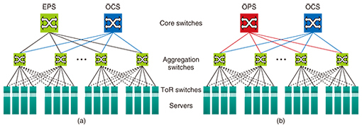
In this article, we present current research trends in photonic DCs. We also introduce a new DC network with a multidimensional torus topology that combines hybrid optoelectronic routers (HOPRs) and an OpenFlow controller. Finally, we highlight the high-speed optical switches that are one of the HOPR’s key enablers used for forwarding incoming packets on a packet-by-packet basis. 2. Expectations for photonic DCsOptical switching technologies used in photonic networks can be divided into optical circuit switching (OCS), optical burst switching (OBS), and optical packet switching (OPS), depending on data granularity. OPS is promising for small-data transmission where data are forwarded on a packet-by-packet basis with low latency and high power efficiency, although the possibility of packet loss is not completely avoidable. OPS is also capable of coping with large traffic fluctuations while maximizing the bandwidth utilization, as a number of optical packets with different destinations can be multiplexed in one wavelength band, which is known as statistical multiplexing. OCS is suitable for large-capacity transmission because it provides reliable links with constant latency and without packet loss. However, it is not suitable for networks in which quick changes occur in the demanded connection paths, as it requires a long setting time to establish a dedicated path at a given wavelength. The amount of research being done on photonic DC networks based on such OCS/OPS technology has recently increased. For example, a network that combines conventional electrical packet switching (EPS) and OCS has been proposed, as shown in Fig. 2(a) [3]. In this network, large-capacity data are forwarded by OCS, making it possible to reduce the end-to-end latency after the links are established and to improve the network throughput by offloading the EPS traffic. Introducing OPS instead of EPS, on the other hand, makes it possible to reduce the latency substantially, even though the paths may be longer compared to OCS, because no time is needed to establish links. Other advantages include reduced power consumption and improved network throughput. For example, a network with a hybrid OPS/OCS configuration has been proposed, as shown in Fig. 2(b) [4]. However, such a hybrid EPS/OCS or OPS/OCS configuration requires separate hardware platforms with different sets of controls.
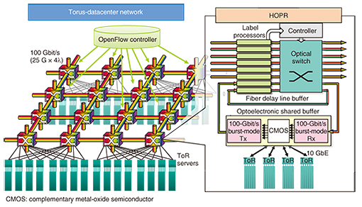
We have proposed a DC network with a torus topology based on the combination of HOPRs and an OpenFlow controller, as shown in Fig. 3. The new flat network provides robust redundancy and superior scalability. In addition, the combination of the OpenFlow-based centralized control and the label processor-based distributed control enables OPS, OCS, and virtual OCS all on a single hardware platform to support a diversity of services in DCs [5]. The HOPR is divided into two parts; one part consists of the optical packet switch that comprises the label processors, optical switch, and optical fiber delay line, and the other part consists of the optoelectronic shared buffer. The HOPR forwards burst-mode 100 Gbit/s (25 Gbit/s × 4λ) optical packets as they are in the optical domain, that is, without performing optical to electrical conversion. However, it is difficult to process such high-speed burst-mode optical packets with the commercially available components and equipment. Therefore, we are developing novel optical and optoelectronic devices in our labs in order to construct a new HOPR prototype that can handle 100-Gbit/s burst-mode optical packets.
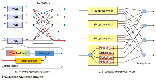
3. High-speed optical switch technologyOne of the key devices in the HOPR is an N×N optical switch that is used for forwarding the incoming optical packets to their desired output ports. Because the data rate of the optical packets is 100 Gbit/s, the length of ordinary Ethernet packets that need to be forwarded is as small as 120 ns. Thus, it is essential to be able to perform switching at a higher speed within the guard bands, that is, the time separating successive packets, which are at least an order of magnitude shorter than the packet length. In addition, the switch needs to be insensitive to bit rate (10–400 Gbit/s), packet format (coherent, wavelength division multiplexing (WDM)), wavelength, and polarization, besides fulfilling other basic demands such as low power consumption, high extinction ratio, low crosstalk, ease of controllability, and compactness. To meet these requirements, various optical switches have been demonstrated so far such as the matrix switches achieved by cascading 1×2 switches, phased-array optical switches, wavelength-routing switches, and broadcast-and-select switches. Of these switches, we consider the wavelength-routing switches and broadcast-and-select switches to be the most promising. The structures of these switches are shown in Fig. 4. The wavelength-routing switch consists of a tunable wavelength converter that changes the wavelength of the input signal light, and an N×N arrayed-waveguide grating (AWG). Since the output port of the N×N AWG is determined by the input wavelength, the AWG enables the input packet to be forwarded to a given output port by converting the packet wavelength to the desired wavelength with a tunable wavelength converter. This kind of optical switch is characterized by high scalability, as it is possible to increase the number of ports N by making the wavelength-channel spacing narrower, without increasing the AWG losses.
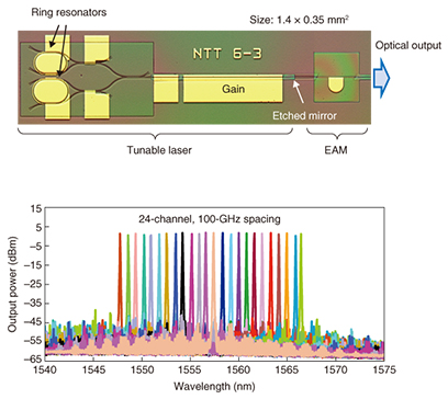
The broadcast-and-select switch, on the other hand, is an optical switch that consists of a 1×N optical splitter and optical gates. The input signal is equally divided by a 1×N optical splitter. Optical switching is done by blocking the light or allowing it to pass using the optical gate attached to the desired output port. This optical switch suffers from limited scalability, though, as the splitting losses increase with the increase in the number of switch ports. It also operates with a simple control for blocking or unblocking the optical gates. Thus, both the wavelength-routing and broadcast-and-select switches have their own merits, and we are conducting research on both of these optical switches. We have proposed a tunable transmitter that relies on a semiconductor ring resonator [6]. A photo of this device is shown in Fig. 5. This device has a tunable laser and optical modulator integrated on a single chip. The tunable laser is promising as a high-speed tunable light source where a low driving current is necessary to change the output wavelength. Moreover, it can suppress the gradual drift in lasing wavelength caused by the Joule heating effect with current injection. The tunable laser employs ring resonators placed in parallel as a wavelength filter for selecting the lasing wavelength and as a loop mirror that forms the laser cavity. With this configuration, it is possible to improve the wavelength selectivity while increasing and stabilizing the optical output. The optical modulator is an electro-absorption modulator (EAM) with InGaAlAs (indium gallium aluminum arsenic)-based multiple quantum wells; it enables operation with a high extinction ratio over a wide range of wavelengths. Using this device and an AWG with 100-GHz channel spacing, we demonstrated error-free wavelength-routed switching for 25-Gbit/s burst-mode optical packets [6].
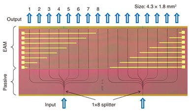
We have also proposed a broadcast-and-select switch based on monolithically integrated EAM gates [7, 8]. A two-array device of 1×8 optical switches is shown in Fig. 6. To compensate for splitting/coupling loss, semiconductor optical amplifiers (SOAs) are usually deployed as optical gates in the broadcast-and-select switches. However, SOAs characteristically experience nonlinear optical effects such as four-wave mixing and cross-gain modulation, and signal-quality degradation for WDM signals is also an issue. An SOA also requires an electrical current of several hundred milliamperes for its operation, which necessitates a driver circuit with high power consumption. Since our alternative choice of an EAM is free from any associated nonlinear effects, and because the device in this case also operates with low current, the power consumption of the driver circuit can be reduced to an extremely low level. The EAM-based switch operates with a normally-on state. Thus, without applying any control signals, the optical signal will go through the bulk active layer that is transparent and polarization-insensitive for a wide range of wavelengths even with a large change in device temperature. In contrast, the SOA-based switch operates with a normally-off state and relies on carrier injection to achieve the on-state necessary for signal transmission. The SOA gain-profile strongly depends on the energy distribution of carriers, which causes its performance to exhibit undesirable changes with wavelength, polarization, or temperature. Thus, in terms of wavelength dependent loss (WDL), polarization dependent loss (PDL), and temperature dependent loss (TDL), the EAM-based switch provides clear advantages when compared to the SOA-based counterpart.
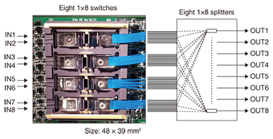
Our fabricated switch module exhibited a small WDL and PDL of typically ± 0.5 dB in the wavelength range of 1540–1560 nm [7, 8]. We have developed a compact 8×8 broadcast-and-select switch module that accommodates eight 1×8 optical switches, as shown in Fig. 7. It exhibits superior properties such as a switching time of no more than 10 ns, a high extinction ratio of at least 40 dB, and power consumption of 3 W or less. We have also achieved error-free forwarding for 25-Gbit/s optical packet signals [9]. This device has excellent low-power, high-speed, and broadband capabilities and is very promising as an optical switch for forwarding large-capacity optical packets since it is compatible with various optical signal formats.
4. Future workWe are currently considering scaling-up the high-speed optical switches (e.g., up to 16×16), and we are also fabricating a pre-prototype HOPR that combines the three basic functionalities of optical label processing, optical switching, and optical buffering. In the future, we plan to build and demonstrate a DC network with a torus topology using the pre-prototype under development, and we will continue our research efforts aimed at realizing environmentally friendly DC networks. AcknowledgmentThis work was partially supported by the National Institute of Information and Communications Technology (NICT). References
|
|||||||||||||||||||