|
|||||||||
|
|
|||||||||
|
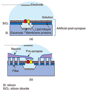
Feature Articles: Forefront Research on Bio-soft Materials Vol. 14, No. 8, pp. 23–27, Aug. 2016. https://doi.org/10.53829/ntr201608fa4 Neuronal Growth on Artificial Structures with Different MaterialsAbstractNeuronal guidance on a device is a key issue to achieve artificial synapses towards the goal of developing artificial post-synaptic structures. NTT Basic Research Laboratories has established a method for examining the in vitro affinity of neurons to a substrate by observing in detail the interface between a neuron and a substrate surface using a focused ion beam/scanning electron microscope at the single neuron level. With this knowledge in hand, we fabricated nanostructures using materials with a high affinity to neurons and examined the ability to control neuronal growth on the structure. We demonstrated the possibility of achieving neuronal guidance on a nanopillar substrate of amorphous silicon, which solves one of several difficulties related to the realization of artificial synapses. Keywords: neuron, FIB/SEM, nanostructure  1. IntroductionRecent advances in nanotechnology and measurement technology have enabled us to obtain highly accurate biological information at high speed. Nanotechnology has been useful not only for diagnostics and treatments but also for developing nanobiodevices, which are nanometer-scale devices with biological functions. Nanobiodevices that utilize the superior functions of biological molecules such as high selectivity and high efficiency have limitless potential for medical care, innovative drug development, and science applications. There are more than 100 billion neurons in a human brain, and they develop their function from a complicated network by delivering signals through synaptic connections. The goal of NTT Basic Research Laboratories is to realize an artificial synapse as a nanobiodevice by mimicking this synapse. A schematic illustration of our artificial synapse is shown in Fig. 1. The artificial synapse can be achieved with neurons forming a synaptic connection with an artificial post-synapse, which can be fabricated by combining nanotechnology and biomolecules. Thus, the mechanism of the brain can be investigated from the signal of each synapse at the molecule and synapse level. For example, we can identify the membrane proteins needed to induce a synaptic connection, and elucidate the mechanism of synapse signal transmission.
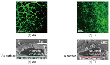
We require various elemental techniques if we are to achieve an artificial synapse. One such technique involves moving neurons towards the artificial post-synapse to achieve a synaptic connection. To do this, it is necessary to prepare an environment in which neurons can grow in vitro to adhere to the substrate, and to elongate the neurites properly. However, to provide an environment for a post-synapse membrane, proteins should be capable of being reconstituted into a lipid bilayer because they can function only when reconstituted into a lipid bilayer in vivo. This means that the device should be covered with a lipid bilayer as shown in Fig. 1(a). However, neurons cannot grow on or adhere to a substrate covered with a lipid bilayer. Therefore, at NTT Basic Research Laboratories, we have proposed nanopillars, which are nanostructures, as a scaffold on which the neurons can grow without adhering to the lipid bilayer (Fig. 1(b)). If neurons grow on nanopillars used as scaffolds, the nanopillars may control the neuronal growth direction, namely providing guidance. We succeeded in evaluating the neuronal affinity with the substrate material at the single cell level by observing their interface by combining a scanning electron microscope (SEM) and a focused ion beam (FIB) to examine the substrate material for neuronal growth control so that the material could be utilized as a nanostructure for a scaffold. Then, with the knowledge we obtained, we showed that neurons grew on the nanostructures by patterning them using the materials for which neurons show high affinity. In this article, we introduce our examination of the interface between neurons and a substrate, and neuronal growth control, namely guidance, using a nanostructure. 2. Evaluation of neuronal affinity and growth with different substratesNeuronal in vitro cultivation has been widely used with the aim of elucidating neuronal signaling mechanisms and for applications in the neural engineering field. Our group has cultivated neurons on various substrates to create interfacial devices for neuronal guidance and thus realize artificial synapses. The interfacial state between neurons and substrates is important information in regard to controlling neuronal growth when we fabricate neuron-integrated devices. Detailed information about the interface between single neurons and substrates, especially nanostructures, can be important in terms of controlling neuronal growth on nanostructured substrates. Several techniques can be used to observe biological samples, ranging from the use of optical microscopes through scanning probe microscopes such as atomic force microscopes. These optical and scanning probe microscopes enable us to observe cell surfaces in detail. However, they cannot be used to directly observe the internal structure of the cells or the interface between the cells and the substrate. NTT Basic Research Laboratories has succeeded in evaluating the interfaces between single neurons and substrates by using FIB milling and subsequent SEM. FIB can process samples by accelerating a gallium ion beam by high voltage [1]. This FIB with an SEM enables us to observe both the cross-sectional and three-dimensional structure of the neurons at a single cell level. In this study, a cell sample was sliced with an FIB/SEM dual system, and its cross-section was observed very precisely [2]. This article introduces the result of observing neurons cultivated on either a gold (Au) or titanium (Ti) substrate obtained with a fluorescent microscope or an FIB/SEM dual system. Neurons were obtained from a rat cerebral cortex. Au has been widely used in the nanotechnology field because its surface chemical characteristics can be modified by functionalizing the surface through self-assembled monolayers of thiols. Ti has superior biocompatibility, and its oxide is used for medical applications such as implants. Thus, the evaluation of the neuronal affinity to different materials can lead to the optimization of neuronal growth scaffolds using nanostructures. Fluorescent images of neurons cultivated on Au and Ti are respectively shown in Figs. 2(a) and 2(b). Green indicates neurons stained with fluorescent dye. A relatively large green grainy lump was observed on the Au, suggesting the aggregation of neurons. In contrast, the neurons on the Ti were observed to be elongated, which means they had dispersed without aggregating. This suggests Ti is more cytophilic than Au. To investigate the neuronal affinity expected from the fluorescent results in more detail, neurons cultivated on Au or Ti were examined using cross-sectional images of the interface between the neurons and the substrate obtained with an FIB/SEM dual system (Figs. 2(c) and 2(d)). The neuron-Au interface exhibited partial adhesion. In contrast, almost all the neurons adhered to the Ti interface. These results are consistent with an assessment made using fluorescence microscopy, and the difference reflects the neuronal affinity of the materials.
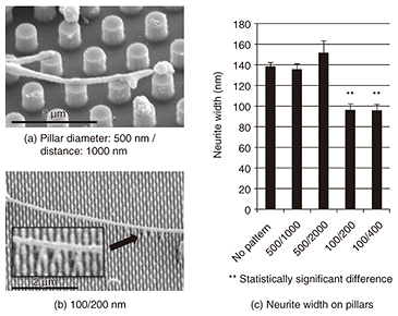
A fluorescent microscope can be used to evaluate the affinity of the multiple cells, but a combination of FIB and SEM can examine the difference in the affinity of a single neuron, and a precise evaluation can be made of the substrate surface. An SEM can provide us with more detailed information because of its much higher spatial resolution, and a detailed interfacial examination will be possible even for nanostructures. In the future, we will aim for an evaluation that includes two-dimensional interfacial mapping and that uses low temperature (cryo) FIB/SEM, which requires fewer samples in the preparation process of fixation and dehydration and thus avoids changing the cellular topologies. 3. Neuronal guidance using nanostructuresNeuronal guidance using nanometer-scale structures including grooves, fibers, and pillars has been attracting attention since the late 2000s, and the structural influences on neuronal adhesion and growth have been examined [3]. However, little attention has been paid to nanostructure materials. As stated above, we examined neuronal affinity with different substrates using the cross-sectional observation of a single neuron. In this section, we examine neuronal growth and guidance capability using nanopillar arrays made of amorphous silicon (a-Si) and Au fabricated as scaffolds for neuronal growth. We fabricated nanopillars 100 and 500 nm in diameter on quartz substrates using electron-beam lithography; then we cultivated rat cortical neurons on them. The samples were then fixed and observed by using either an SEM or confocal laser scanning microscope (CLSM) after the treatment. The first process in the treatment was fixation to stabilize the protein, which is the main structural molecule of the cell. Thus, the observed cell structures resembled their intact structures after fixation. The sample for SEM observation was further dehydrated and freeze-dried, and the sample for CLSM was also immunostained to identify the specific protein localization. SEM images of neurites (axons or dendrites) elongated from neurons cultivated for 7 days on a-Si nanopillars are shown in Fig. 3. The neurites were observed to adhere to the nanopillars, and they grew on pillars with diameters of 500 and 100 nm. Some of the narrower pillars were bent by the neurite growth (magnified in the inset in Fig. 3(b)).
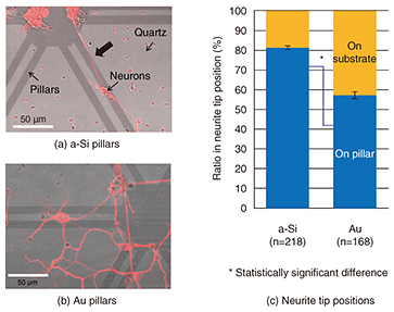
By comparing the widths of neurites cultivated on different nanopillar patterns, we found that the neurites were significantly wider on wider-diameter pillars (Fig. 3(c)). Neurites on the wider pillars were almost as wide as neurites on a plane substrate. This suggests that the size of the neuronal adhesion area affects neurite width. The neuronal width can be determined by the adhesion area; a neurite adhering to a substrate promotes the expression of cytoskeletal proteins. This result shows that 500-nm-diameter pillars allow neurites to grow in the same manner as on a plane substrate. Then, we examined neurons on different pillar materials, as shown in Fig. 4. Neurons grew longer along with the patterns on a-Si pillars (Fig. 4(a), thick arrow) while they elongated randomly on both Au pillars and a quartz substrate (Fig. 4(b)). A quantitative analysis revealed that there was a higher ratio of neurite tips on the a-Si pillars than on the Au pillars (Fig. 4(c)) [4]. This low affinity of neurons for Au corresponds to neuronal cross-section results obtained using FIB/SEM. These results demonstrate the possibility of achieving neuronal guidance using nanopillars made of appropriate materials.
4. Realizing an artificial synapseWe established a method of evaluating the in vitro neuronal affinity to a substrate with different materials using a single neuron by observing neuronal cross-sections. Furthermore, we demonstrated the possibility of controlling the neuronal growth using nanopillars made of high affinity materials. The neuronal growth direction can be controlled by controlling the nanopillar array. Then, neurons can be expected to grow towards the device, namely the artificial post-synapse, which would be fabricated in advance. Thus, in the future, we will investigate the mechanism of synaptogenesis by realizing an artificial synapse by the bottom-up examination of molecules; for example, the identification of proteins (synaptogenesis factors) for synapse formation. AcknowledgmentsThis work was supported by Grants-in-Aid for Scientific Research (KAKENHI; Grant Number 15H03541) from the Japan Society for the Promotion of Science. References
|
|||||||||