 |
|||||||||||
|
|
|||||||||||
|
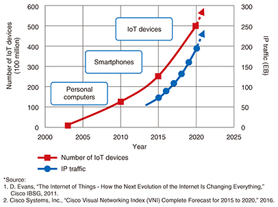
Feature Articles: Photonics-electronics Convergence Devices that Support AI-IoT Service Era Vol. 15, No. 1, pp. 6–10, Jan. 2017. https://doi.org/10.53829/ntr201701fa1 On Si Platform Opens a New World in AI-IoT Service EraAbstractIn the near future, ICT (information and communication technology) services are expected to achieve a dramatic evolution through the use of the cloud, IoT (Internet of Things), and AI (artificial intelligence). The communication devices necessary to realize this new era require high performance, high functionality, low cost, and low power consumption. A fusion of various technologies and know-how will be applied in order to meet these requirements. In this article, we explain the concept of an on Si platform, which expands upon silicon (Si) photonics, as one solution. We also show the direction of research and development (R&D) of various elemental technologies and describe the R&D fabrication process to realize the on Si platform concept. Keywords: device technology, transceiver, Si photonics 1. IntroductionThe Internet of Things (IoT) is the internetworking of physical devices, vehicles, buildings, and other items that are embedded with electronics, sensors, actuators, and network connectivity that enable these objects to collect data, which are then stored in datacenters. The second-order information obtained by analyzing the real-time data will have great value. In the near future, even this kind of data analysis will be done by artificial intelligence (AI) rather than by people, and this AI will make it possible to create high quality services, bring changes in lifestyle, and boost economic activity. Some of the expected changes in the number of IoT devices and amount of IP (Internet protocol) traffic are shown in Fig. 1. Some reports predict that by 2020, at least 25 to 50 billion things will have been connected to the Internet [1, 2]. The huge number of things connected to the Internet will lead to an explosive increase in traffic. This will present certain challenges for the NTT laboratories conducting research and development (R&D) on optical devices.
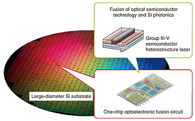
The first challenge concerns the economic element of the increased traffic volume. Mobile traffic, including that of the IoT, is expected to be about 1000 times larger in volume in 2025 compared to 2010, as shown in Fig. 1. Capital investment is necessary in order to meet the demand of the sharp increase in traffic. However, we must avoid passing on the cost to users. Thus, that same 1000-times (or higher) increase in communication traffic must be implemented at lower cost. The second challenge concerns the size of optical devices. As mentioned above, the traffic volume is expected to be 1000 times larger by 2025. If the size of the optical devices used then is the same as that of the current ones, 1000 times more capacity will be needed for accommodating optical devices, which is not realistic. Therefore, there is strong demand for smaller and more highly integrated optical devices. The last challenge concerns power consumption. Data collected by IoT devices will be stored in datacenters. However, the power consumption of datacenters in 2018 is expected to account for 3% of total power consumption worldwide. The huge use of power has become a serious problem that needs to be solved on a global scale in order to avoid global warming. The NTT laboratories are focusing on the use of silicon (Si) platform technologies as the direction of research to solve these challenges in the AI-IoT service era. 2. On Si platform technologyMost electronic appliances such as personal computers and smartphones use electronic devices such as LSIs (large-scale integrated circuits) and integrated circuits (ICs) that contain silicon (Si), one of the most common semiconductors. In the electronic device field, Moore’s law states that the integration density of Si ICs doubles every 1.5 years. This tremendous progress is expected to be continued in the fabrication process of Si wafers as the wafer diameter increases. The nanofabrication and high integration of the transistor bring higher device performance and also push down the unit cost of the transistor. In contrast, most optical devices such as laser diodes (LDs) and photodiodes (PDs) consist of III-V semiconductors such as indium phosphide. With optical devices, nanofabrication and high integration would not necessarily bring high performance and lower cost devices as with electronic devices. Optical devices are fabricated on smaller III-V semiconductor-based wafers, and elements such as the LDs and PDs are each assembled with lens or with optical isolators, which increases the assembly cost. The high assembly cost prevents us from developing less expensive and highly integrated devices. If we could successfully fabricate optical devices by using a similar process to that of electronic devices with the larger Si-based wafers, we could solve the three challenges described above. The NTT laboratories are working on a novel technology called on Si platform technology that combines the fabrication process of electronic devices on larger Si wafers with optical III-V semiconductor technology. On Si platform technology is the concept to achieve ultra-small, low-cost, and low-power-consumption devices compared to previous optical devices. The proposed technology (Fig. 2) is a fusion of the fabrication techniques used in the fields of electronic devices and optical devices that NTT laboratories have developed up to now. This technology enables us to fabricate devices with greater economic efficiency (low cost) that also have a level of functionality and performance that cannot be realized using only Si-based materials by integrating optical and electronic devices on a Si wafer.
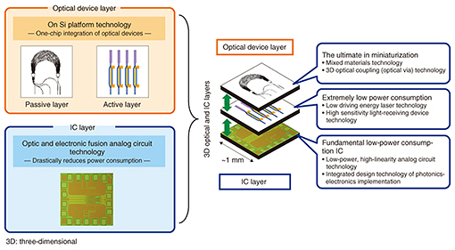
Much research has been done throughout the world in an attempt to produce a low-cost optical device and ultimately realize an optical circuit (Si photonics) by using the manufacturing method used in the field of electronic devices. However, the fusion of Si photonics and optical semiconductor technology that provides the laser and the receiver has not yet reached a satisfactory state. Therefore, the NTT laboratories are trying to develop a Si platform by accumulating know-how of semiconductor crystal growth and process technologies and by extending Si photonics. An example of on Si platform technology developed as a proof of concept in the NTT laboratories is a 1-mm2 transceiver chip, as shown in Fig. 3. This ultimate device integrates functions for both transmitting and receiving data within a tiny area. Although it is difficult to integrate all functions within 1 mm2, we nevertheless refer to this device as a 1-mm2 transceiver, as we are optimistic that it will be realized.
This 1-mm2 transceiver consists of three layers and uses stacking technology. The first layer is a passive layer that can perform the splitting, demultiplexing, or phase control of the light on a Si wafer. The second one is an active layer that includes the LDs with extremely low power consumption. The third one is the IC layer that controls optical devices such as the LDs and PDs. Stacking technology is used to integrate the electrical and optical binding into a three-dimensional (3D) configuration. Many challenges are involved in each layer to realize the 1-mm2 transceiver. In the passive layer, a technique to form a light coupling in the vertical direction (optical via) is necessary in order to avoid the limitations of size. In the active layer, very low power consumption should be achieved without any optical degradation. In the IC layer that controls the optical devices, even though the previous electronic circuits were designed to have general versatility, a total redesign of the electronic and optical devices is needed in the 1-mm2 transceiver. Furthermore, the propagation distance of the high-speed signal to be integrated into the 3D configuration needs to be shorter. This will result in lower cost and more compact devices while improving the performance. 3. R&D foundry for optical devices in the futureIn the electronic device field, production facilities are expensive to build and maintain. The enormous cost can be a drain on the finances of the company that owns them. To avoid such huge costs, economic forces have led to the existence of many companies that only design devices, which are called fabless semiconductor companies, as well as foundries that only manufacture devices without designing them. In the field of Si photonics devices, some foundries that only manufacture optical devices have already started operations, as in the electronic device industry. However, in the optical device field, production systems are not well equipped. In particular, foundries that can manufacture wafers consisting of Si material and the compound semiconductors used in LD and PD fabrication have not yet been established. Therefore, the NTT laboratories aim to play a key role in Japan, and even in the world, as an R&D foundry for optical devices consisting of Si photonics, compound semiconductors, and electronic devices. To support the R&D, we are steadily accumulating and preparing for the fusion of a variety of technologies and knowledge for the coming AI-IoT service era. 4. Future developmentAs described in this article, on Si platform technology using extremely small, low cost, and low power devices is expected to open the door for new AI-IoT services. To address the three issues mentioned in section 1, the NTT laboratories are promoting the development of this technology and planning for a timely release on the market of the devices developed using it. The Feature Articles in this issue introduce the recent progress in basic element technologies to realize a 1-mm2 transceiver by using on Si platform technology. Specifically, the articles introduce optical waveguide technology for ultra-compact, high-density integration [3], LD and PD technology for low power consumption and miniaturization [4], and ultra-low-power analog IC technology [5]. References
|
|||||||||||

