|
|||||
|
|
|||||
|
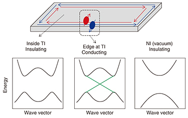
Feature Articles: A New Era in Quantum Information Processing Technologies Vol. 15, No. 7, pp. 28–32, July 2017. https://doi.org/10.53829/ntr201707fa6 Creating New Two-dimensional Topological Insulators for Fault-tolerant Quantum ComputingAbstractTwo-dimensional topological insulators (2DTIs) pave the way to explore novel quasiparticles for fault-tolerant quantum computing and to create devices utilizing spin degree of freedom. However, host materials that realize 2DTIs have so far been limited to two systems. In this article, we propose a strained quantum well structure as a new 2DTI candidate and demonstrate that strain enhances the energy gap and leads to superior bulk insulation properties. Keywords: two-dimensional topological insulators, fault-tolerant quantum computing, strain band engineering  1. IntroductionTopological insulators (TIs) featuring insulating bulk and conducting edge states originating from topologically nontrivial inverted band structures have been attracting much interest. Topology is a field of mathematics; objects with shapes that can be made to conform to each other by a continuous deformation are said to have the same topology. TIs are insulators but have a different topology than normal insulators (NIs), as their band structures cannot be transformed continuously into each other [1]. Therefore, at the interface between a TI and NI (which includes a vacuum), the band gaps must close, which results in conducting edge states at the interface (Fig. 1). The Nobel Prize in Physics 2016 was awarded to US scientists for “Theoretical discoveries of topological phase transitions and topological phases of matter.” This further fueled research interest in topological materials science.
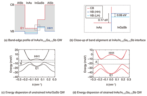
TIs were first proposed for two-dimensional (2D) systems. The theory predicted ballistic and quantized transport at the edge of TIs. Moreover, helical spin current in which the spin direction is locked to the direction of momentum (e.g., up spins to the left and down spins to the right) was predicted. The helical spin current can be used as a spin source with semiconductors to create novel spintronic devices. Additionally, it is theoretically predicted that Majorana fermions show up in topological superconductors where the edge states of a TI are proximitized by a superconductor. Majorana fermions have a different nature than conventional particles of fermions and bosons, and they are promising for use in fault-tolerant quantum computing because they are protected from most types of decoherence. Thus, TIs have been proposed as a platform for exploring spintronic applications and exotic quasiparticles. In this article, we introduce a strained quantum well (QW) structure as a new 2DTI candidate and demonstrate that strain enhances the energy gap and leads to superior bulk insulation properties [2]. 2. New 2DTI candidateAlthough various materials have been theoretically proposed as 2DTI candidates, experimental reports of transport properties clearly indicative of 2DTIs have so far been limited to two systems, cadmium telluride/mercury telluride (CdTe/HgTe) QWs and indium arsenide/gallium antimonide (InAs/GaSb) QWs, both of which are lattice-matched semiconductor heterostructures. Historically, the CdTe/HgTe system was first predicted to be a 2DTI, which was subsequently followed by the InAs/GaSb system. InAs and GaSb are conventional semiconductor materials that are easier to work with than HgTe. The InAs/GaSb system has a key advantage of being in situ tunable between normal and topological insulating phases. However, the residual bulk conductivity in the topological insulating phase has been an obstacle to investigating edge transport. In this article, we propose InAs/indium gallium antimonide (InGaSb) strained QWs as a new 2DTI candidate that can overcome this problem. 3. Strain band engineeringThe band-edge profile of an InAs/In0.25Ga0.75Sb strained QW is shown in Fig. 2(a). Electrons and holes are separately confined to the InAs and In0.25Ga0.75Sb QWs, where they form subbands E1 and HH1, respectively. The conduction band (CB) bottom of InAs is located ~0.17 eV below the valence band (VB) top of In0.25Ga0.75Sb (Fig. 2(b)). Note that this ordering of the band extrema is opposite to that in ordinary semiconductors. This band inversion is a prerequisite for topological insulators. Additionally, In0.25Ga0.75Sb has a larger lattice constant than aluminium antimonide (AlSb), which induces compressive strain in the In0.25Ga0.75Sb layer. This splits the VB edge of the heavy hole (HH) and light hole (LH) by 0.06 eV (Fig. 2(b)), strengthening (weakening) the interaction between CB and HH (LH). From these relations, we expect larger band inversion for strained InAs/InGaSb QWs than unstrained InAs/GaSb QWs. We calculated the energy dispersion relation by using the k・p method because the energy gap Δ originating from the interaction between E1 and HH1 opens at a finite wave vector k. The band structure of an unstrained InAs/GaSb QW is shown in Fig. 2(c) in comparison to that of a strained InAs/In0.25Ga0.75Sb QW (Fig. 2(d)) for InAs and (In)GaSb thicknesses of 10 and 6 nm, respectively. As the calculations show, the InAs/In0.25Ga0.75Sb strained QW has larger band overlap and larger Δ than the unstrained InAs/GaSb QW, suggesting favorable bulk insulation properties in the strained InAs/InGaSb QW.
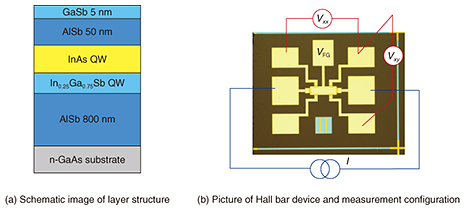
The heterostructures studied were grown by molecular beam epitaxy on Si (silicon)-doped (001) GaAs substrates (Fig. 3(a)). The QWs consist of InAs and 5.9-nm-thick In0.25Ga0.75Sb, sandwiched between AlSb barrier layers. Four heterostructures with different InAs layer thickness (8.5, 9.1, 10.0, 10.9 nm) were prepared. The heterostructures were processed into Hall bar devices (width: 50 μm, voltage-probe distance: 180 μm) by using lithography (Fig. 3(b)). We applied current I and obtained longitudinal resistance Rxx from voltage Vxx and Hall resistance Rxy from voltage Vxy. Gate voltage VFG was used to vary the carrier density. Magnetic field B was applied perpendicular to the sample plane.
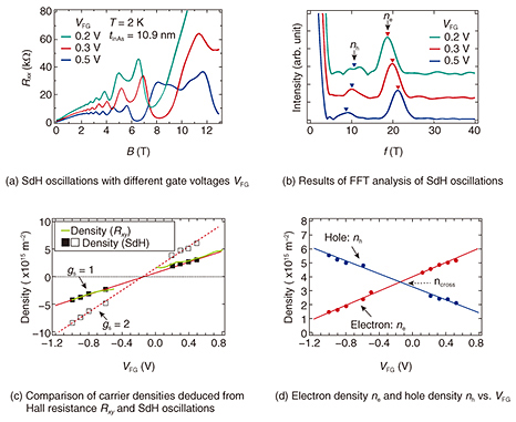
4. Quantitative analysis of band inversionIn Fig. 4(a), Rxx vs. B is plotted for different VFG values at 2 K. The sample contained a 10.9-nm-thick InAs QW. Due to the quantization of cyclotron motion of electrons and holes by a strong magnetic field, Rxx oscillates as a function of B (SdH (Shubnikov-de Haas) oscillation). Fast Fourier transform (FFT) analysis of the SdH oscillations revealed two frequency components f (Fig. 4(b)). The one with the corresponding carrier density increasing (decreasing) with VFG can be identified as being associated with electrons in InAs (holes in InGaSb). The coexistence of electrons and holes indicates that the band is inverted and the Fermi level intersects both electron-like and hole-like bands. Carrier density n is related to f as n = gsf(e/h). Here, h is Planck’s constant, e is elemental charge, and gs is spin degeneracy. Moreover, gs can take a value of 1 or 2; gs = 1 (2) means that the energy levels are spin-split (degenerate). To determine whether gs = 1 or 2, we compared the total carrier densities deduced from Rxy with those deduced from SdH oscillations for both spin-degenerate and spin-split cases. Interestingly, we found the energy levels were spin split (gs = 1) in the InAs/InGaSb strained QW (Fig. 4(c)). Such characteristics have not been observed in the conventional InAs/GaSb QWs. One possible origin of the spin splitting is spin-orbit interaction; however, further investigation is necessary to clarify the origin. A quantitative measure of band inversion is given by kcross [= (4πncross/gs)1/2], the wave vector at which the anti-crossing of E1 and HH1 occurs. From the linear fit of the dependence of electron density ne and hole density nh on gate voltage (Fig. 4(d)), we obtained the density ncross at the charge neutrality point (where ne = nh) of 3.6 × 10¹⁵ m−2. Using the ncross and gs values, we obtained kcross = 0.21 nm−1.
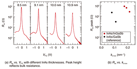
5. Enhanced bulk resistivityThe Rxx peak height at the charge neutrality point measured at 0.25 K, which mainly reflects in-gap states in the bulk, increased with decreasing InAs thickness and reached 889 kΩ (corresponding resistivity of ~10 h/e2) for the 8.5-nm-thick QW (Fig. 5(a)). Higher peak resistance indicates superior bulk insulation properties. The obtained Rxx peak values are plotted as a function of kcross (Fig. 5(b)). The data for InAs/GaSb QWs are also plotted as a reference. The InAs/InGaSb strained QWs exhibited higher bulk resistivity in the deep band inverted regime than that of the reference. Generally, the residual bulk conductivity problem becomes more significant as the band inversion increases. Therefore, it was hard to satisfy high bulk resistivity and deep band inversion at the same time with unstrained InAs/GaSb QWs. The k・p calculation predicts that an even larger energy gap can be obtained by exploiting higher strain, that is, a higher In composition in the InGaSb layer. This means that there is much room to improve the bulk insulation properties by optimizing the strained QW structure.
6. ConclusionHigh bulk resistivity in the deep band inverted regime was obtained by using InAs/InGaSb strained QWs. Our results demonstrate that InAs/InGaSb strained QW structures are a promising platform for robust 2DTIs, where intrinsic edge physics can be studied with the advantage of good bulk insulation deep in the band-inverted regime. As the next step, we plan to demonstrate quantized edge transport by optimizing InAs/InGaSb strained layer structures. The origin of the spin-splitting transport properties should also be clarified. Demonstration of the quantized edge transport in strained QWs will be an important step in studies of superconductor/TI heterojunctions for fault-tolerant quantum computing. References
|
|||||