|
|||||||||||||||||||||||||||||||||||
|
|
|||||||||||||||||||||||||||||||||||
|
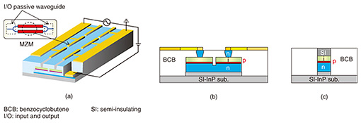
Regular Articles Vol. 16, No. 4, pp. 49–56, Apr. 2018. https://doi.org/10.53829/ntr201804ra2 High-speed Modulator for Next-generation Large-capacity Coherent Optical NetworksAbstractModulators with very high speeds are necessary to achieve the next-generation of 1-T/λ coherent optical networks. In this article, we describe our recently developed InP (indium phosphide)-based in-phase and quadrature (IQ) modulators with ultrahigh bandwidth and low half-wavelength voltage (Vπ). We utilize a structure with extremely low electrical loss and obtain a 3-dB electro-optic bandwidth of over 67 GHz without degrading other characteristics such as driving voltage and optical loss. The IQ modulator performs IQ modulation at up to 120 Gbaud without optical and electrical pre-equalization. Furthermore, we developed an ultralow power modulator driver employing 65-nm CMOS (complementary metal-oxide semiconductor) technology and fabricated an IQ modulator co-assembled with this driver IC (integrated circuit), and successfully demonstrated 64-Gbaud/16QAM (quadrature amplitude modulation) operation. Keywords: InP-based modulator, digital coherent technology, high-speed modulation  1. IntroductionOptical transport networks require more channel capacity and greater flexibility in the modulation format in order to cope with the ever-growing global IP (Internet protocol) traffic [1, 2]. Digital coherent optical transmission technology is a key for increasing the capacity of optical networks. The Optical Internetworking Forum (OIF) is discussing a polarization-division multiplexing in-phase and quadrature (IQ) modulator with high bandwidth and flexible modulations for 400 and 600 G/λ, such as 64 Gbaud/16 quadrature amplitude modulation (16QAM) and 64 Gbaud/64QAM. Moreover, much higher baud-rate modulation targeting 1-T/λ, for example, 100 Gbaud/32QAM and 100 Gbaud/64QAM, has been demonstrated in the research phase [3, 4]. To achieve the high-speed, high-order modulation format and low power consumption, it is necessary to improve modulator performance with regards to the electro-optic (EO) bandwidth, half-wavelength voltage (Vπ), and the optical insertion loss of the modulators. To extend the transmission distance, a higher baud rate is preferred over higher-level modulation [5]. For example, the transmission distance of a 128-Gbaud/quadrature phase-shift keying (QPSK) signal is theoretically more than twice that of a 64-Gbaud/16QAM signal. Thus, a higher bandwidth modulator is a key component for the next-generation of metro-regional area and long-haul transmission networks. Moreover, optical transceivers tend to have low power consumption and small footprints. Therefore, it is very important to achieve a high bandwidth modulator with a low Vπ. Lithium niobate (LiNbO3: LN)-based modulators have been used in digital coherent systems, and they now support baud rates of up to 64 Gbaud (3-dB bandwidth: ~35 GHz, Vπ: ~3.5 V). However, further extending the bandwidth and reducing the Vπ of LN modulators is challenging due to the material properties. In contrast, indium phosphide (InP)-based Mach-Zehnder modulators (MZMs) and IQ modulators have several excellent features for achieving high speed and low Vπ (3-dB bandwidth: ~40 GHz, Vπ: < 2.0 V). For example, InP-based MZMs exploit the quantum-confined Stark effect and use waveguides with strong optical confinement, which are beneficial for reducing the driving voltage with a short interaction length. Several high-speed InP IQ modulators with a capacitive-loaded traveling-wave electrode (CL-TWE) design have been reported [6–10]. The CL-TWE allows the optimization of the EO frequency response for high baud-rate applications because its design flexibility enables us to achieve low radio frequency (RF) loss, impedance matching, and velocity matching between RF and optical signals. InP IQ modulators can perform modulations at up to 100 Gbaud [4]; however, the rate of 100 Gbaud has not been exceeded yet. A bandwidth of over 60 GHz is ideally needed for operations at rates beyond 100 Gbaud. Reducing the EO interaction length is one way to extend the EO bandwidth; however, Vπ is increased [9, 10]. An effective way to overcome this trade-off and to achieve both higher speed and lower Vπ in InP-based modulators is to reduce the series resistance of the semiconductors. Namely, since a p-doped InP layer has about one order of magnitude higher bulk and contact resistivity than those of an n-doped InP layer, reducing the resistance of the p-doped cladding layer is a promising way to extend the EO bandwidth without increasing the Vπ and the optical propagation loss. In this article, we introduce our recent work on ultrahigh-bandwidth InP IQ modulators with a low Vπ and low optical loss. By employing a new n-i-p-n heterostructure—where a thick p-doped cladding layer replaces a thick n-doped layer and a thin p-doped layer—and a conventional CL-TWE, we have developed a modulator with an extremely low electrical loss. The device exhibits a 3-dB EO bandwidth of over 67 GHz and a Vπ of less than 1.5 V. We demonstrated 120-Gbaud QPSK modulation toward achieving ultrahigh-speed operation [11]. Furthermore, we developed the most power-efficient MZM driver using complementary metal-oxide semiconductor (CMOS) technology and demonstrated 64-Gbaud/16QAM operation with ultralow power dissipation by co-assembling the driver integrated circuit (IC) with our IQ modulator [12]. 2. Modulator designIn this section, we describe our modulator design for achieving a much higher EO bandwidth. Schematic illustrations and cross-sectional diagrams of the fabricated MZM are shown in Fig. 1. We found that we could improve the bandwidth further by replacing the thick p-doped (conventional) over-cladding layer with an n-doped layer. For that reason, we employ an n-i-p-n heterostructure; namely, an n-doped InP lower cladding layer, a thin p-doped layer, an undoped core layer (InGaAlAs/InAlAs (indium gallium aluminium arsenide and indium aluminium arsenide) multi-quantum well), and an n-doped InP upper cladding layer are grown on an InP (100) semi-insulating (SI) substrate. The thin p-doped layer acts as an electron carrier blocker, which enables us to apply voltage efficiently across the undoped core layer. The modulator has an inverted trapezoidal ridge waveguide in the modulation region and a deep-ridge waveguide in the I/O (input and output) passive waveguide region, as shown in Fig. 1(b) and (c), respectively. The inverted trapezoidal ridge shape has the potential to achieve lower contact resistivity and parasitic capacitance, which provides more bandwidth improvement than a trapezoidal ridge shape. The n-doped upper cladding layer in the non-modulation region is replaced with an SI cladding layer to achieve electrical isolation and a lower optical propagation loss. These waveguides are formed along the [011] stripe direction to obtain a synergistic EO effect [13]. The [011] direction waveguide also enables us to fabricate an inverted trapezoidal ridge shape by chemical wet etching.
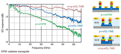
The EO response of our newly developed n-i-p-n structure MZM with CL-TWE is shown in Fig. 2. The EO responses for conventional p-i-n structure MZMs are also given for comparison. Utilizing the n-i-p-n structure makes it possible to greatly reduce the series resistance of the MZM. In addition, the CL-TWE potentially has a low electrical loss and offers flexibility in terms of optimizing the impedance and microwave velocity. As a result, we can extend the EO bandwidth further; in fact, we achieved an EO bandwidth of over 67 GHz (1.5-GHz reference).
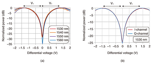
3. Basic IQ modulator characteristicsIn this section, we describe the characteristics of the IQ modulator. 3.1 Static characteristicsThe DC (direct current) extinction characteristics at wavelengths between 1530 and 1560 nm are shown in Fig. 3. The Vπ is less than 1.5 V, and the static extinction ratio (ER) exceeds 24 dB for all the sub-MZMs and the entire C-band, as shown in the figure. We confirmed that the ER characteristics had good uniformity. The fiber-to-fiber optical insertion loss at peak transmission was less than 9 dB, which includes the coupling loss of lensed fibers (~3.5 dB/facet). The on-chip loss was estimated to be approximately 2 dB, which is equivalent to that of an InP MZM formed with a passive waveguide. This indicates that the absorption loss of the thin p-cladding layer is negligibly low, and the optical loss of our waveguide is lower than that of a conventional p-i-n waveguide.
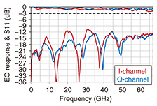
3.2 High-frequency responsesWe measured the small-signal high-frequency characteristics. In this experiment, the 50-Ω termination chip resistors were flip-chip bonded on a die, which has the advantage of eliminating the parasitic inductance caused by gold (Au) wire bonding and improving the impedance matching [14]. This configuration contributes to improving the EO bandwidth and reducing the electrical reflections (S11). The measured EO responses and S11 are shown in Fig. 4. The measured 3-dB EO bandwidth for all channels exceeded 67 GHz, which was the limit of the measuring instrument. The electrical reflection was less than –10 dB, which is small enough for practical use. These results indicate that our IQ modulator meets the requirements for both a high-speed response and low-drive voltage by the use of a low-loss waveguide configuration and an optimized electrode design. Furthermore, we believe that the flip-chip configuration is a promising approach for high baud-rate operation compared with conventional RF-terminating connection techniques such as Au-wire bonding.
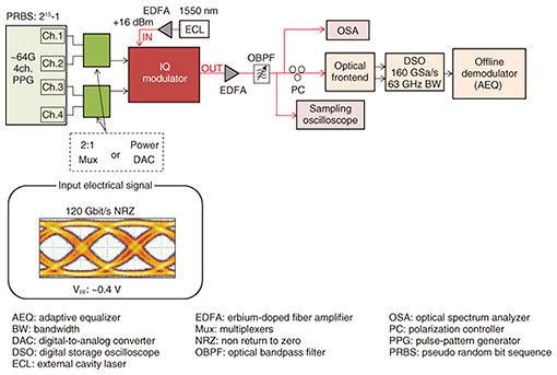
4. Single-IQ modulator characteristicsWe also investigated the dynamic characteristics of our IQ modulator. The modulator was driven as a single-ended drive for 80- and 120-Gbaud QPSK modulations. The experimental setup for IQ modulations is shown in Fig. 5. We used an external cavity laser (ECL) with a < 30-kHz linewidth as the signal light source. The wavelength and power of the optical input were 1550 nm and +16 dBm, respectively. An up to 64-Gbit/s quad-channel pulse-pattern generator (PPG) was used as an electrical signal source. For 80- and 120-Gbaud QPSK signals, we used high-speed 2:1 multiplexers with an output voltage of ~0.4 Vpp, and multiplexed the electrical signals from the PPG into 80-Gbit/s and 120-Gbit/s signals.
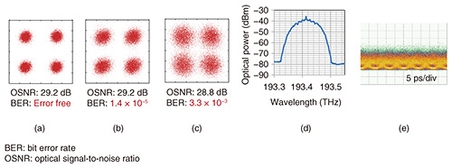
The generated electrical signals are shown in Fig. 5. These signals with a PRBS (pseudo random bit sequence) of 215-1 were then fed into the modulator via a multiport RF probe. The modulated optical signals were amplified by an EDFA (erbium-doped fiber amplifier) and passed through a 100-GHz optical filter. On the receiver side, we used a single-polarization offline coherent receiver consisting of an optical frontend, a DSO (digital storage oscilloscope) with a sampling rate of 160 GSa/s and an analog bandwidth of 63 GHz, and an offline demodulator, where we used an AEQ (adaptive equalizer). We also observed the modulated signals using an OSA (optical spectrum analyzer) and a sampling oscilloscope with an unfiltered optical bandwidth of 65 GHz. The back-to-back constellation diagrams for 80-Gbaud QPSK and 120-Gbaud QPSK signals are shown in Fig. 6(a), (b), and (c). Clear constellations were obtained for all modulations. We estimated the bit error rate (BER) for up to 120-Gbaud QPSK modulations, with the modulator driven directly by the multiplexer signals (without RF amplifiers), because no amplifier supporting a 120-Gbaud rate was available. We achieved error-free 80-Gbaud QPSK generation at the optical signal-to-noise ratio (OSNR) of 29.2 dB as shown in Fig. 6(a). We also evaluated the modulation without equalization and obtained a BER of 1.4 × 10⁻⁵ as shown in Fig. 6(b), when the length of the finite impulse response filter was set at 1. In the 120-Gbaud QPSK modulation, the BER at an OSNR of 28.8 dB was 3.3 × 10⁻³, which is still below the limit of the soft-decision 20%-overhead forward error correction in 400G systems. The optical waveform and spectrum of the generated 120-Gbaud QPSK signal are respectively shown in Fig. 6(d) and (e). Although the driving voltage was insufficient for a full swing condition (2 Vπ), a clear 120-Gbaud rate modulation was confirmed. These results indicate that our modulator has an ultrahigh bandwidth characteristic. We can improve the BER characteristics by using an ultra-broadband amplifier and obtaining an adequate modulation depth.
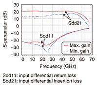
5. Driver IC co-assembled IQ modulator characteristicsFor short reach applications such as metro-regional areas and transmission links between datacenters, small pluggable digital coherent transceivers with lower power consumption are needed. To meet this demand, we have developed modulator drivers with ultralow power dissipation, because a large portion of power for transceivers is consumed by driver ICs. We utilize a stacked current mode architecture and an open-drain structure to achieve the lower power consumption [15]. To obtain a wide bandwidth, three-dimensional inductors were used for the inductor peaking techniques [16]. Our modulator driver was fabricated using 65-nm CMOS technology. When the driver drives a 50-Ω impedance load, the consumed power is only 180 mW. The measured differential S-parameters (scattering parameters) at the maximum and minimum gain settings are shown in Fig. 7. At the maximum gain setting, the 3-dB bandwidth and the differential gain are 56.2 GHz and 20.8 dB, respectively. At the minimum gain setting, they are 60.6 GHz and 12.9 dB, respectively.
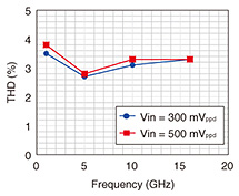
Single-tone sine wave responses were measured to evaluate the linearity of the driver. The measured total harmonic distortion (THD) versus frequency at an output swing of 2 Vppd is plotted in Fig. 8. From a 300- to 500-mVppd input swing and in a 1- to 16-GHz frequency range, the THD remains less than 4%.
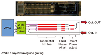
A microscopic image and a schematic diagram of the fabricated IQ modulator co-assembled with the dual-channel CMOS differential driver IC we developed are shown in Fig. 9. The differential drive scheme provides the IQ modulator with both lower power operation and broadband pure push-pull (zero chirp) drive [17]. In the experimental setup, we used an arbitrary waveform generator with a sampling rate of up to 92 GSa/s (Keysight M8196A) as a signal source, and an optical modulation analyzer (OMA) (Keysight N4391A OMA) on the receiver side. In addition to the OMA, we used an offline demodulator for BER measurements as well as for the single-IQ modulator evaluation. Similarly, other instruments in our setup such as the ECL and the optical filter were also the same as those for the previous experiment.
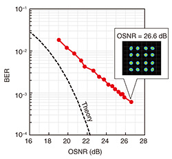
The measured single-polarization 64-Gbaud/16QAM constellation diagram and the back-to-back BER as a function of the OSNR are shown in Fig. 10. We obtained a clear constellation and a BER of less than 10−2 for an OSNR of more than 20.3 dB. The OSNR penalty from the theoretical limit at a BER of 10−2 was approximately 2.3 dB. The difference is mainly due to the performance limitations of the experimental instruments and imperfect adjustment of the IQ modulator driving condition. The consumed power of the two channels of the driver IC was only 495 mW. These results indicate that we have attained a driver IC power dissipation of less than 1 W for dual-polarization IQ modulation in 400-G/λ systems.
6. ConclusionWe described an ultrahigh bandwidth and low-Vπ InP IQ modulator with an n-i-p-n heterostructure. The device exhibited a 3-dB EO bandwidth of over 67 GHz, a Vπ of less than 1.5 V, and low optical loss operation. We obtained clear IQ modulation signals at a rate of up to 120 Gbaud without optical pre-equalization. Furthermore, we developed the most power-efficient modulator driver—a 56-GHz-bandwidth 2.0-Vppd linear modulator driver employing 65-nm CMOS technology—and succeeded in demonstrating 64-Gbaud/16QAM operation by co-assembling the driver IC with an IQ modulator chip on a carrier. We believe our low electrical and optical loss modulator is suitable for both ultrahigh speed and ultralow power modulation for use in next-generation coherent transmitters. References
Trademark notesAll brand names, product names, and company names that appear in this article are trademarks or registered trademarks of their respective owners. |
|||||||||||||||||||||||||||||||||||