|
|||||||||||||||||||||||||
|
|
|||||||||||||||||||||||||
|
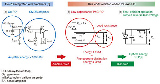
Feature Articles: Forefront of Research on Integrated Nanophotonics Vol. 16, No. 7, pp. 8–13, July 2018. https://doi.org/10.53829/ntr201807fa2 Ultralow-capacitance Optoelectronic Converters Using a Photonic CrystalAbstractThe fusion of optical technology and electronic circuitry is the key to increasing capacity in any type of information processing, but optoelectronic integrated processing on a chip requires compact and energy-efficient photodetectors (optical-to-electrical (OE) converters) and optical modulators (electrical-to-optical (EO) converters). This article introduces such OE/EO converters that are implemented using a photonic crystal nanostructure and thus feature low capacitance and an extremely low energy cost. Keywords: photonic crystal, photodetector, optical modulator  1. IntroductionOptical technology has played an important role in the optical transmission of information in telecommunication and data communication. Consequently, there is currently a demand for optical technology for communication over ultrashort distances (millimeter order) within computing chips and for the computational processing itself [1]. There is thus a need for combining optical technology with mature complementary metal-oxide semiconductor (CMOS) integration technology, and recent research on the fabrication and integration of small optical elements on silicon substrates has been vigorous. However, conventional optical elements, and particularly optoelectronic converters such as optical transceivers, are large and consume large amounts of energy. Therefore, cost-performance is significantly low when such elements are connected to CMOS circuits for on-chip computation applications, so a fundamental change in the elemental devices such as photodetectors (optical-to-electrical (OE) converters) and optical modulators (electrical-to-optical (EO) converters) is needed. Since most optoelectronic conversion devices include semiconductor p-i-n (p-type, intrinsic, n-type semiconductors) junctions and metal electrodes, the devices themselves have a certain capacitance component. In the case of a photodetector (PD), absorption of light produces a charge (Q) on its capacitance (C), and a voltage (V) is generated for driving the electronic circuit. Although there are various operating principles for a modulator, one involves modulating light by applying voltage to produce a charge (Q) on capacitance (C) to create an electric field within the structure. In any case, with the relationship Q = CV, the required charge Q can be reduced by lowering the capacitance and operating voltage of the device, thus reducing energy consumption. For that purpose, it is necessary to restrict the light to as small an area as possible to enable a strong interaction of light and material. An effective means of achieving this is to use a nanostructure. At NTT, we have succeeded in developing PDs and modulators that can operate with low latency and extremely low capacitance by combining the nanostructure known as a photonic crystal (PhC) with an indium phosphide (InP) semiconductor, a material that has been important in the manufacture of optical communication devices, for which NTT has excellent fabrication technology. 2. Photonic-crystal photodetector (PhC-PD)Conventional PDs incorporate a transimpedance amplifier (TIA) to generate the voltage required by the electronic circuit after the photocurrent Ipd is produced by light absorption (Fig. 1(a)) [2]. However, such devices have major problems when there is dense integration on chips, including high energy consumption on the order of 100 fJ/bit, as well as having a large footprint and delay. Structural simplification can be considered for PDs that are more energy-efficient, and one approach is to connect a high load resistance Rload to the PD for a simple configuration that performs light-to-voltage conversion, where the generated voltage is given by V = IpdRload (Fig. 1(b)). In this case, there is a trade-off in that the light-to-voltage conversion efficiency is proportional to the load resistance Rload, but the operating band is inversely proportional to the RC time constant, so this approach is not feasible for conventional devices. To achieve high performance in both aspects at the same time requires reduction of the device capacitance C, and if that problem can be solved, an amplifier-free PD may be possible. At NTT, we are working toward developing such a PD by using a PhC nanostructure [3].
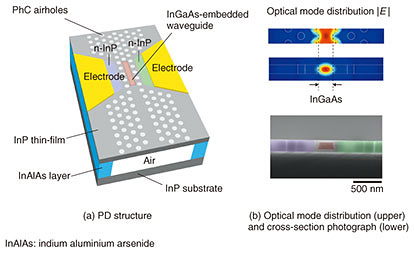
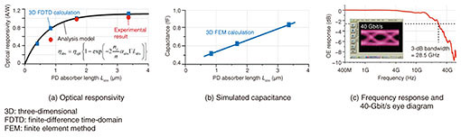
The PhC-PD structure is illustrated in Fig. 2(a). The two-dimensional array of airholes that constitute the PhC strongly confine light within the waveguide because of the periodicity of the large refractive index difference, so various kinds of optical devices can be made smaller. The key steps in the fabrication of PDs are the embedding of an indium gallium arsenide (InGaAs) light absorption layer in an InP thin-film (250 nm thick) using highly precise semiconductor embedding heterostructure fabrication technology and the formation of a PhC with high positioning accuracy by electron-beam lithography and plasma etching [4]. As shown by the cross-section photograph in Fig. 2(b), a compact light absorber is formed within a PhC waveguide, and the PD is successfully fabricated by forming lateral p-i-n junctions. The strong light confinement in the PhC waveguide provides sufficient light absorption efficiency to enable an optical responsivity of 1 A/W even in an extremely short PD length (1.7 µm) (Fig. 3(a)). This structure of a thin-film and short PD length sandwiched between a low-dielectric-constant material (air) makes it theoretically possible to suppress the capacitance of the p-i-n junctions to 0.6 fF (Fig. 3(b)). Also, the dynamic characteristics (frequency response in the 28.5-GHz operating band and the eye diagram for a 40-Gbit/s optical signal) reveal that sufficiently high efficiency and high speed are both achieved, even with such an ultrasmall PD (Fig. 3(c)).
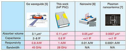
The performance of various small PDs is compared in Table 1. While our PD has about the same high optical responsivity and operating bandwidth as the germanium PDs that are being actively researched based on a silicon photonics platform [5], it also achieves an ultrasmall absorption layer and ultralow capacitance, features contributed by the nanostructure PD. Nanowire [6] and plasmon antenna structures [7] also hold promise for miniaturization, but improvement of light responsivity is currently a problem. We therefore consider the PD described here as the most balanced candidate.
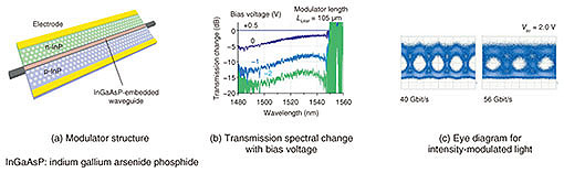
We have investigated light-to-voltage conversion with a circuit in which our PD was connected to a kΩ-order load resistor. Measurements of the voltage generated at the load resistor revealed high conversion efficiency of up to 4 kV/W, which is similar to or higher than that achieved with a PD that integrates an amplifier. Although the operating bandwidth is limited to several gigabits per second because of the parasitic capacitance of the metal wiring, the operation at 40 Gbit/s is possible when considering the theoretical PD capacitance of 0.6 fF. Photodetection while connected to such load resistance can be considered a step towards an amplifier-free photoreceiver. We have also recently discovered the possibility of achieving a bias-free PD. Conventional PDs apply an external reverse bias voltage to the p-i-n junctions for fast response. In that case, however, the power consumption corresponds to the product of the photocurrent and the bias voltage. Ideally, PD operation without bias is desirable, and if it can be achieved together with the amplifier-free operation described above, an extremely low-power-consumption PD that operates on optical energy alone can be expected (Fig. 1(c)) [8]. The problem is that when a high load resistance connection is considered, a forward voltage that corresponds to the generated voltage is applied to the PD. Although that is in the same current-voltage operating region as solar cells, high-speed operation on the gigahertz order is not expected because high-speed carrier transport is difficult. With our PD, however, high-speed operation can be expected even under forward voltage because of the efficient absorption and carrier extraction in the depletion layer that are enabled by the narrow waveguide cross-section (Fig. 1(b)). Actually, operation at a high speed of 20 Gbit/s and high responsivity has been observed, even with a forward voltage of +0.4 V applied. This feature is not seen with conventional PDs. These results suggest the feasibility of an extremely small, energy-efficient photoreceiver that operates on ultralow optical energy of about 1 fJ/bit. 3. PhC optical modulatorOptical modulators, which do the reverse of PDs by converting an electrical signal to an optical signal, must also be made small and energy-efficient for implementation in photonic integrated circuits. For the optical pass-gate logic circuit that we propose, low latency is essential, and hence, a short length is required [9]. NTT has also fabricated a small electro-absorption modulator (EAM) that employs PhC fabrication technology in the same way as the PD described above (Fig. 4) [10]. The embedded layer is composed of InGaAsP (indium gallium arsenide phosphide), which has an absorption wavelength of 1.45 µm. Applying a reverse voltage produces the Franz-Keldysh effect*, increasing light absorption to modulate the output light intensity. In the experiment, high-speed optical modulation such as the eye diagram for 40-Gbit/s and 56-Gbit/s signals was obtained.
Research has been done on EAMs that use SiGe (silicon germanium) or other such core material on a silicon substrate for application as on-chip optical modulators [11]. Such devices require a high reverse bias voltage (> 4 V), and the high energy dissipation (7 fJ) due to the photocurrent from absorption and the bias voltage has been a significant bottleneck. Our PhC EAM averts that problem because it operates on a low reverse bias voltage (–0.2 V), significantly reducing energy dissipation (0.2 fJ). At the same time, the low charging energy of 1.6 fJ/bit due to the device capacitance (13 fF) and signal voltage (0.7 V) results in an operating energy of 1.8 fJ, which is much lower than that for conventional devices. In practice, incident light energy is also required for optical transmission, so in the future we will need to conduct an overall evaluation in an optical transmission system that takes the optical energy required on the PD side into account.
4. OutlookWe have described optoelectronic conversion at an overwhelmingly lower operating energy than is possible with conventional technology and is achieved with small PDs and EAMs that employ PhC nanostructures. We can expect that future development will go beyond these single devices and achieve multi-functionality through integration. For example, the short-distance optical link for transmitting the signal between the modulator and the receiver is promising for application to high-speed data sharing within many-core chips. The O-E-O optical wavelength converter fabricated by close integration of the PD and modulator for transferring the optical signal to a different wavelength light is also possible. The extremely low operating energy compared to conventional devices enabled by the technology described here is a major differentiating factor, and application to on-chip optical signal routing and optical computing by combining the functions can be expected. References
|
|||||||||||||||||||||||||