|
|||||||||||
|
|
|||||||||||
|
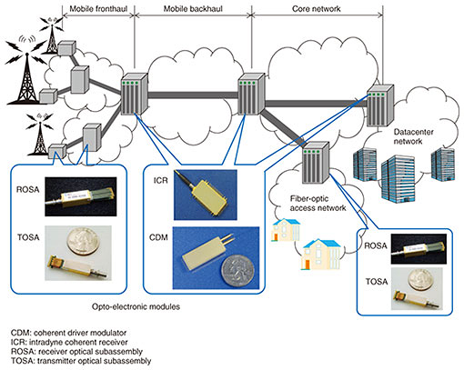
Regular Articles Vol. 17, No. 4, pp. 21–27, Apr. 2019. https://doi.org/10.53829/ntr201904ra1 Simulation Technology for Analysis and Virtual Fabrication of High-speed Opto-electronic ModulesAbstractIn the last decade, demand for high-speed data transmission has been growing dramatically not only for datacenter traffic but also for mobile and fiber-optic access networks. To meet the demand, NTT Device Innovation Center (DIC) has been developing opto-electronic modules, including a receiver optical subassembly, transmitter optical subassembly, intradyne coherent receiver, and a coherent driver modulator. NTT DIC has been working to accelerate the deployment of these opto-electronic modules on actual fiber-optic networks and has developed technology enabling full-digital virtual fabrication of high-speed opto-electronic modules on computer. In this article, we describe the latest simulation technology, focusing in particular on the opto-electronic modules and their capabilities and performance. Keywords: opto-electronic modules, simulation, virtual fabrication, 5G mobile networks, fiber-optic access networks  1. IntroductionFiber-optic data transmission technology is crucial for building both long-haul and short-haul transmission networks. For instance, as traffic on mobile and fiber-optic access networks continues to escalate, the capacity of both short- and long-haul fiber optic networks should be increased simultaneously. Recent aggressive investment in the fifth-generation wireless communication (5G) networks has become the key factor in regard to accelerating this undeniably strong trend in optical-fiber cable manufacturing and network expansion. According to an announcement made by the Georgia Department of Economic Development last year [1], the manufacturing capacity of optical fiber cables by a major global optical fiber manufacturer was predicted to double by the end of 2019 in order to cope with the rapidly expanding deployment of 5G mobile fronthaul and backhaul networks. The basic architecture of 5G mobile and fiber-optic access networks is shown in Fig. 1. In the next few years, optical transceivers with the capacity for high-data-rate transmission will be fully deployed on these networks.
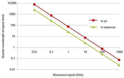
Moreover, additional trends are occurring with the optical transceiver segments. A large number of million-scale optical transceivers are used in fiber-optic networks. Thus, optical transceivers are essentially key components enabling high-speed conversion between optical signals and electrical signals. Furthermore, with requirements to downsize optical transceivers, increase data rates, and reduce power dissipation, the optical transceiver has to simultaneously attain high speed, miniaturization, and integration. However, some natural laws that limit downsizing make these improvements difficult, especially in opto-electronic modules such as receiver optical subassemblies (ROSAs) [2], transmitter optical subassemblies (TOSAs) [3], intradyne coherent receivers (ICRs) [4], and coherent driver modulators (CDMs) [5], which are installed in the optical transceivers. As data speeds increase, opto-electronic modules come under more stress and exhibit signal power loss and crosstalk aggression from densely packed opto-electrical and microwave parts due to natural electromagnetic effects. These natural electromagnetic phenomena degrade the signal integrity performance of the opto-electronic modules. Therefore, cut-and-try methods are commonly adopted in the actual development stage for downsizing. However, in view of the limited resources available for simultaneous development of various types of opto-electronic modules, it is imperative to break away from conventional development methodologies and to develop a novel procedure in the face of such inherently complicated limitations. This is our primary reason for pursuing the development of full-digital virtual fabrication on computer. 2. Preliminary analysis in signal integrity issuesVarious optical transceivers and related opto-electronic modules such as ROSAs, TOSAs, ICRs, and CDMs, which were described in the previous section, are used in fiber-optic transmission networks. These opto-electronic modules are being miniaturized, and therefore, designers of optical modules need to concentrate on maintaining signal integrity performance in relation to electromagnetic issues. The relationships between signal speeds and their quarter-wavelength in a microwave region are shown in Fig. 2. The quarter-wavelength rule is well known in the field of microwave design, and this must also be taken into account when building these opto-electronic modules. In the case of a 100-Gbit/s (25 Gbit/s x 4-lambda) TOSA [2], the package width is approximately a few millimeters, which is almost the same as the quarter-wavelength of 25 Gbit/s, as shown in Fig. 2. Generally, the TOSA is assembled with many different parts, including electro-absorption modulator integrated distributed feedback (EA-DFB) lasers, microwave components, and direct current (DC) power delivery parts. All the signal nets and DC power drains are accommodated densely in one package. The high-density assembly easily induces crosstalk aggression due to coupling between adjacent signal nets, as well as microwave resonance and ground bouncing if quarter-wavelength microwave rules are not taken into account when designing the modules.
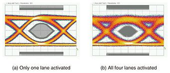
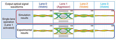
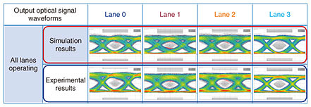
Eye diagrams when only a single lane or all four lanes were activated are shown in Fig. 3. In this case, each lane corresponds to a different signal net in the TOSA. As shown in the figure, there was relatively strong distortion when all four lanes were activated. However, the geometric structures in the open part of both eyes were almost the same. There were no crushing deformations in the center of the eye diagram even under the four-lane operating condition. The remarkable differences between the two cases were the eye opening ratio and the amount of amplitude distortion at high level, which determined the signal-to-noise ratio. Generally, under the condition of crosstalk aggression between different adjacent channels, eye diagrams of victim channels are distorted around the center of the eye diagram, and the shape changes from its original shape to a triangle or another geometrically complicated shape. Therefore, improving the eye diagrams in this TOSA was not as simple as just reducing the crosstalk between different adjacent channels. We had to take microwave resonance and ground bouncing into account while paying attention to quarter-wavelength rules caused by high density assembly in a small package.
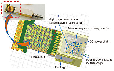
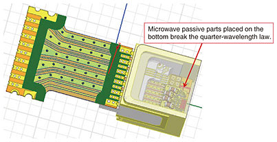
3. Modeling and simulatingAs discussed, there is a strong trend toward miniaturizing the size of optical modules. Thus, conventional deployment methodologies such as cut-and-try are not appropriate due to limitations of free space for assembly modifications in small packages. To achieve a breakthrough to meet this challenge, we built a novel full-digital optical module simulator by combining and modifying different commercial microwave simulators. This newly developed simulator is capable not only of showing dynamic characteristics in small-signal and large-signal analyses, including eye diagram output functions, but also of indicating areas of signal integrity degradation on a three-dimensional (3D) model. A simulation model of the 100G TOSA is shown in Fig. 4. As demonstrated in this model, four lanes were tightly assembled in one package with many microwave passive components, DC power drain parts, and EA-DFB lasers.
Eye diagrams and crosstalk aggression optical signals at a victim lane are shown in Fig. 5 with one lane activated in the TOSA. Eye diagrams with all four lanes activated are shown in Fig. 6. As shown in Figs. 5 and 6, all of the simulation results correlated relatively well with the experimental results. Moreover, this simulator identified the root cause of the signal integrity distortion in the 3D model. We confirmed that there was an area with ground-bouncing noise located in the deep part of the TOSA package on the 3D model. This area apparently had a unique structure, which broke the quarter-wavelength rules.
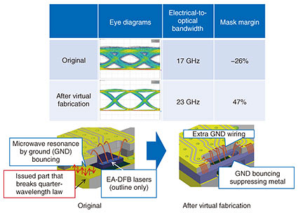
4. Virtual fabricationAs described in the previous section, this newly developed simulator successfully identified the root cause of signal integrity distortion in the TOSA. Moreover, the capabilities of the 3D-model simulating functions enable this simulator to virtually fabricate optical modules on a computer. After the first simulation, we found that a microwave passive component, which broke the quarter-wavelength law, was initiating the ground bouncing, as shown in Fig. 7. With the conventional cut-and-try methodology, it is impossible to rapidly modify or replace the parts since the allocated place is nearly at the bottom of the TOSA. In contrast, our simulator rapidly and easily solved this problem. After the 3D modeling of a correct microwave part, we were able to fabricate a new TOSA virtually.
Eye diagrams of the original conditions and the virtually fabricated TOSA are shown in Fig. 8. A new piece of metal was placed on the ground-bounced microwave parts, and the microwave resonance between two microwave parts was successfully suppressed by the virtual fabrication. As can be seen in Fig. 8, large modification of the TOSA was not necessary to obtain the eye diagram. Thus, both the simulation technology and the virtual fabrication technology enabled us to minimize time and costs effectively during our opto-electronic module development at NTT Device Innovation Center.
5. Conclusion and future prospectsWe described newly developed simulation technology used for studying and developing opto-electronic modules, focusing in particular on a 100-Gbit/s (25 Gbit/s x 4) TOSA. This simulation technology features not only dynamic performance analysis but also virtual fabrication on a computer. This technology is expanding the scope of our opto-electronic module development, which involves ROSAs, ICRs, CDMs, and other types of modules, and successfully shortening the development period. We also plan to build high-performance computing systems enabling the simulation and virtual fabrication of beyond-100-GHz-bandwidth opto-electronic modules. References
|
|||||||||||