|
|||||||||||||||||||||||||||
|
|
|||||||||||||||||||||||||||
|
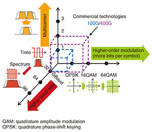
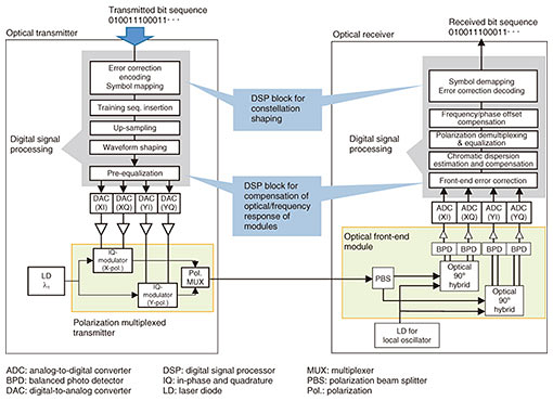
Feature Articles: Ultrahigh-speed Transmission Technology to Support High-capacity Communications Infrastructure of the Future Vol. 17, No. 5, pp. 12–19, May 2019. https://doi.org/10.53829/ntr201905fa2 Ultrahigh-speed Optical Communications Technology Combining Digital Signal Processing and Circuit TechnologyAbstractThis article introduces ultrahigh-speed optical communications technology that achieves the optical transport networks needed to support an advanced information society. Most data traffic is carried on the Ethernet; 400G Ethernet has recently been standardized, and discussions have also started on standardizing signal speeds in excess of 1 Tbit/s. This technology is used to economically transmit high-speed client signals such as Ethernet signals on optical fiber networks. The combination of advanced digital signal processing and ultrahigh-speed circuit technology can greatly improve the speed and quality of optical signals and is expected to result in cost-efficient ultrahigh-speed optical communications at rates in excess of 1 Tbit/s per channel. Keywords: optical communications, digital signal processing, high-speed Ethernet  1. IntroductionUltrahigh-speed optical communications technology is the fundamental technology that determines the transmission performance of optical networks. In a backbone network, multiple ultrahigh-speed client signals such as 400G Ethernet (400GE; standardized in 2017) are accommodated in high-speed optical channels based on digital coherent transmission technology [1], and multiple high-speed optical channels are combined by wavelength division multiplexing (WDM) to implement a long-distance high-capacity optical network. Meanwhile, the rate of internal data transmission between servers in datacenters that support various services such as social networking and video distribution services is becoming very large, and so is the demand for communications between multiple datacenters. Compared with the backbone network, the transmission distances are shorter, but greater economy is required, and high-speed data transmission is implemented by employing a technique called intensity-modulation direct-detection (IM-DD), which has a simple transceiver configuration. 2. Technical issues in increasing the optical signal data rateOptical communications technology capable of accommodating 100-Gbit/s and 400 Gbit/s client signals per channel has already been put to practical use [2]. During the Ethernet standardization activities, discussions were initiated and are continuing on the next transmission speed standard, with 800 Gbit/s and 1.6 Tbit/s being cited as possible candidates. In the future, optical networks are expected to accommodate high-speed client signals at speeds of over 1 Tbit/s per channel. The three key elements of high-speed optical signals are shown in Fig. 1. Conventional IM-DD systems transmit information using binary light intensity signals (either on or off), but by using the digital coherent technique shown in Fig. 2, it is now possible to use optical amplitude and phase information to transmit signals with four or more values per pulse. In addition, by performing digital signal processing in the transceiver, it is possible to equalize and compensate for wavelength deformation caused by polarization separation and wavelength dispersion and polarization mode dispersion that occur inside the optical fibers, resulting in substantial increases in the transmission range and data transmission rate.
Currently, practical optical signals carrying data at a rate on the order of 100 Gbit/s per channel are achieved by using polarization multiplexing to combine 4-value quadrature phase-shift keying (QPSK) signals at a rate of 32 Gbaud. In addition, 400-Gbit/s optical signals are achieved by using two carriers (wavelengths) to carry two 16-quadrature amplitude modulation (QAM)*1 polarization multiplexed signals at 32 Gbaud in a single transmission channel. There are also three key elements for speeding up optical signals (Fig. 1). The first is to use a higher baud rate (light pulse speed). If the baud rate is increased, this provides a corresponding increase in the transmission rate per wavelength. If signals have the same number of bits per symbol, then the baud rate can be increased without any excessive deterioration of reception sensitivity, but in order to transmit and receive these high baud rate signals, it is necessary to use devices that are capable of operating at high speed, including electrical devices such as digital-to-analog converters (DACs), analog-to-digital converters (ADCs), and optical devices such as optical modulators and balanced photo detectors (BPDs). Also, in the frequency domain, the bandwidth occupied by optical signals increases in proportion to the baud rate. This means that fewer signals can be combined by WDM, so unless this approach is combined with the use of a higher number of bits per symbol as described later, the overall capacity of the transmission system will not increase. The second element is the use of more bits per symbol. By increasing the number of optical amplitude levels and phases used for signal transmission, it is possible to increase the number of bits that can be transmitted in a single optical pulse. For a given baud rate, the transmission speed improves in proportion to the number of bits per symbol*2. With more bits per symbol, devices such as DACs and ADCs must have greater resolution and linearity, and the required signal-to-noise ratio (SNR) also increases. This decreases the maximum transmission distance, and reduces the resilience to signal distortion. Although QAM with a square constellation is currently used, it is possible to improve the required SNR by using a modified constellation. The third element is the use of multicarrier transmission. By configuring one channel from optical signals of multiple wavelengths (carriers), it is possible to increase the capacity per channel in proportion to the number of carriers. This is an effective method for configuring a logical high-speed channel in an optical network. For example, it is possible to achieve a channel speed of 1 Tbit/s by bundling five 200-Gbit/s per wavelength optical wavelengths at different wavelengths into a single channel. However, since this increases the required number of transceivers, the abovementioned increases in baud rate and number of bits per symbol result in a higher transmission rate per wavelength but require the application of multicarrier technology that takes transmission performance and economy into consideration. Thus, in order to attain ultrahigh-speed optical transmission at rates in excess of 1 Tbit/s per channel, it is essential to increase the baud rate and the number of bits per symbol, and while developing high-speed devices, it is necessary to use highly sensitive digital signal formatting and signal processing technology that enable the device requirements to be relaxed.
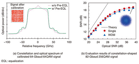
3. Digital calibration technology and high-sensitivity technology to maximize device performanceSignal degradation may occur when transmitting and receiving high-speed signals, even if the bandwidth of the electrical device or optical device meets the respective requirements. For example, as shown in Fig. 2, a digital coherent transmitter requires four DACs and two IQ (in-phase and quadrature) modulators for each polarization component. The receiving side requires four BPDs and four ADCs. Due to differences such as variations within manufacturing tolerances, the characteristics of these devices and the connections between them may not necessarily be uniform when they are all interconnected. These sorts of errors can have a major impact on the signal quality of high baud rate signals and signals with a large number of bits per symbol. At our laboratory, we have managed to achieve substantial improvements in signal quality by digitally correcting device imperfections on the receiving side, and by using digital signal processing on the transmitting side to perform ultra-precise pre-equalization and calibration of the frequency characteristics and variation of devices in the transmitter. The optical spectrum of a 64-Gbaud 64QAM signal before and after calibration is shown in Fig. 3(a). Pre-equalization smooths out the optical spectrum and improves its quality so that the indistinct signal constellation is resolved into a set of 64 clearly distinguishable points [3]. Also, with regard to the loss of sensitivity at a higher number of bits per symbol, we are studying how the signal constellation can be adapted in order to increase the signal sensitivity. Conventionally, multilevel QAM signals such as QPSK, 16QAM, and 64QAM have used signal constellations in which every point appears with equal probability. Although a multilevel QAM signal can be generated from the original bit sequence by using simple mapping and demapping processes, this does not yield an optimal signal constellation from an information theoretical point of view. Attention has recently been focused on information-theoretical signal point-shaping techniques that can be used to achieve near-optimal signal constellations by arranging the constellation points of multilevel QAM signals based on probability distributions. Although this technique requires dedicated mapping and demapping processes, it enables the same number of data bits to be transmitted with a lower minimum SNR than that of multilevel QAM. Also, since the number of data bits to be transmitted can be changed by changing the probability distribution of constellation points without changing the base multilevel QAM signal, there is no need to modify the signal processing algorithm used for modulation and demodulation. Our laboratory has conducted a successful test demonstration of 800 Gbit/s per wavelength transmission by using this pre-equalization calibration technique and 256QAM-based constellation shaping as shown in Fig. 3(b) [4]. With this technique, an optical network can use one or two wavelengths to accommodate client signals of 800 Gbit/s and 1.6 Tbit/s, which are candidate data rates for the next-generation Ethernet standard.
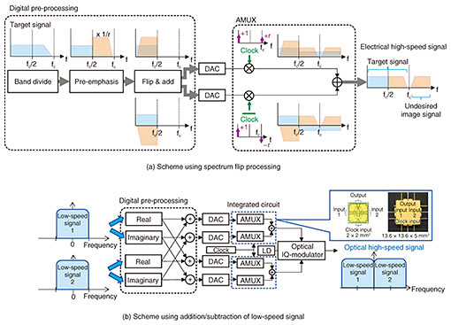
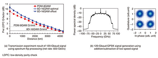
4. Bandwidth doubling technology for high-speed signal generationOne of the most important devices for generating high-speed optical signals is the DAC. DACs are integrated with digital signal processing LSIs (large-scale integrated circuits), but the analog bandwidth of DACs fabricated using Si CMOS (silicon complementary metal oxide semiconductor) is currently around 40 GHz. While the above calibration technique enables some correction, it becomes a bottleneck at high baud rates beyond 100 Gbaud. Our laboratory proposed bandwidth doubling technology that can double the analog bandwidth of a DAC. This technology involves preliminary signal processing of the desired wideband signal and outputting signals from two DACs. Using an analog multiplexer (AMUX) circuit [5] to combine these signals makes it possible to generate high-speed signals with twice the bandwidth. We proposed the two bandwidth doubling methods shown in Fig. 4, and by applying these two methods to digital coherent transmission technology, we conducted an experimental demonstration of ultrahigh baud rate signal transmission using DACs with a 32-GHz analog bandwidth. We show in Fig. 5(a) the results of a transmission experiment using a 120-Gbaud signal generated using the spectral method shown in Fig. 4(a). In this experiment, we successfully transmitted data at a net rate*3 of 600 Gbit/s per wavelength over a long distance of approximately 4000 km [6]. Also, for the addition/subtraction processing method shown in Fig. 4(b), we made a prototype circuit integrated with two AMUX circuits, and we successfully generated 120-Gbaud QPSK signals as shown in Fig. 5(b) [7].
In theory, it is difficult to generate high-quality signals at 100 Gbaud or above using 40-GHz DACs, because the DACs require a bandwidth of at least half the baud rate. With our technique, it is possible to extend the bandwidth of existing DACs, enabling the signal baud rate to be increased. In addition, by combining the abovementioned calibration and sensitivity enhancement techniques, we have found that it is possible to achieve ultrahigh-speed signal transmission at over 1 Tbit/s per wavelength without resorting to multicarrier technology [8].
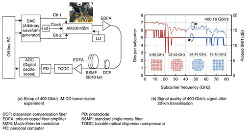
5. Application of ultrahigh-speed optical communications technology to short-distance communicationsThe simple and highly economical system configuration of the IM-DD method has attracted attention as an optical communications technique for short-distance communications on the order of a few tens of kilometers at most, where most traffic occurs between servers or between datacenters. The recently standardized 400GE system uses PAM4 (4-level pulse amplitude modulation) to produce four parallel 100-Gbit/s signals per wavelength and thus requires four sets of transceiver equipment. At our laboratory, we have performed successful short-distance transmissions over 20 km at a bit rate of 400 Gbit/s using a single transceiver by combining bandwidth doubling technology with an ultra-wideband indium phosphide (InP) modulator [9, 10]. This is the world’s highest transmission rate for IM-DD using a single wavelength and a single polarization. The results of this transmission test are shown in Fig. 6. In this experiment, we used an InP optical modulator with an exceptionally wide bandwidth together with a bandwidth doubler to generate a wideband electrical signal and were able to generate optical signals while maintaining the wide bandwidth of the electrical signal. Also, by using DMT (discrete multitone) as the modulation method, we generated 256 subcarrier signals by digital signal processing, and by allocating appropriate signal bits to each carrier according to the frequency characteristics of the electrical and optical devices, we achieved near-optimal bit allocation.
For example, as shown in Fig. 6(b), a high-SNR 6.96-GHz subcarrier is used for 64QAM signals, and a low-SNR 9.10-GHz subcarrier is used for 16QAM signals. The use of bandwidth doubling technology and a wideband modulator has made it possible to allocate even multilevel signals such as 16QAM to the high frequency domain. With this technology, it is expected that transmission rates of over 400 Gbit/s per wavelength can be achieved by IM-DD with a simple and economical transceiver configuration. 6. SummaryIn this article, we introduced ultrahigh-speed optical transmission technology that combines digital signal processing and high-speed circuit technology to achieve optical networks that will form the infrastructure of an advanced information society. We have shown that this technology is capable of ultrahigh-speed optical transmission at over 1 Tbit/s per wavelength. In the future, we will keep working on improving the speed and will continue with our research and development so that this technology can provide a highly reliable communications infrastructure. References
|
|||||||||||||||||||||||||||