|
|||||||||||||||||||
|
|
|||||||||||||||||||
|
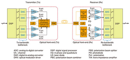
Feature Articles: Ultrahigh-speed Transmission Technology to Support High-capacity Communications Infrastructure of the Future Vol. 17, No. 5, pp. 27–33, May 2019. https://doi.org/10.53829/ntr201905fa4 Ultrahigh-speed Optical Front-end Device Technology for Beyond-100-GBaud Optical Transmission SystemsAbstractTo support sustainable progress of optical communications, intense research and development (R&D) is being conducted to expand the transmission capacity per channel (transmission capacity per wavelength). Beyond-100-GBaud high-symbol-rate optical transmission technology is now attracting a great deal of attention for its use in constructing future cost-effective optical transport networks. This article introduces recent trends and challenges in optical communications and presents NTT’s recent R&D in ultrahigh-speed optical front-end device technology for beyond-100-GBaud systems. Keywords: high-symbol-rate optical transmission, bandwidth doubler, optical front-end device  1. Trends and challenges in optical communicationsThe amount of data traffic in optical communications networks continues to grow exponentially due to the spread of broadband applications and services such as video streaming, cloud computing, and IoT (Internet of Things). In particular huge-capacity and long-haul transmission technology is required in the core network in order to accommodate client data and to link metropolitan areas. Novel digital coherent technology, which combines coherent detection and digital signal processing, has been deployed to cope with such rapid growth in communications traffic [1]. To date, 100-Gbit/s-per-channel (wavelength) systems based on 32-GBaud polarization division multiplexing (PDM) quadrature phase-shift keying and 400-Gbit/s-per-channel systems based on two-subcarrier 32-GBaud PDM 16-ary quadrature amplitude modulation (16QAM) have been put into practical use. In the future, transmission capacity per channel is expected to exceed 1 Tbit/s to handle the ever-growing communications traffic. The transmission capacity can be increased by increasing the symbol rate, increasing the modulation order, or adding more subcarriers. Increasing the symbol rate is the most advantageous approach from the viewpoint of ensuring both cost effectiveness and transmission distance. Therefore, high-symbol-rate beyond-100-GBaud optical transmission technology is now attracting a great deal of attention for its use in constructing future optical transport systems with capacities exceeding 1 Tbit/s per channel. Researchers face several challenges in constructing an optical transceiver enabling beyond-100-GBaud systems. A block diagram of a conventional optical transceiver for digital coherent systems is shown in Fig. 1. To construct a 100-GBaud system, each building block in the transceiver needs to have at least a 50-GHz analog bandwidth, which is the Nyquist frequency of 100 GBaud. One of the biggest challenges is finding a way to overcome the analog-bandwidth limitation of digital-to-analog converters (DACs) and analog-to-digital converters (ADCs), which are fabricated using Si (silicon) complementary metal oxide semiconductor (CMOS) technology.
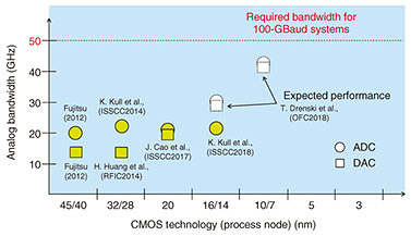
The analog-bandwidth performance of cutting-edge CMOS-based DACs and ADCs is shown in Fig. 2. This graph indicates that it is very hard for CMOS-based DACs and ADCs to satisfy the target analog-bandwidth of over 50 GHz. One more unavoidable challenge is determining how to integrate and assemble optical front-end devices—modulator drivers (DRVs) and optical modulators on the transmitter side and trans-impedance amplifiers and photodiodes on the receiver side—into a packaged module to avoid a degradation in quality of beyond-100-GBaud signals due to extra loss derived from packaging. Hence, integration and packaging technology becomes much more important in beyond-100-GBaud systems.
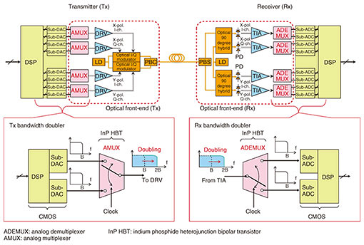
2. Bandwidth doubler technologyWe have devised novel bandwidth doubling technology to overcome the analog-bandwidth limitation of CMOS-based DACs and ADCs [2]. A block diagram of an optical transceiver applying the bandwidth doubler is shown in Fig. 3. On the transmitter side, two pre-processed analog signals from CMOS-sub-DACs are multiplexed into one double-bandwidth signal by the analog multiplexer (AMUX). On the receiver side, one broadband signal is demultiplexed into two half-bandwidth signals by the analog demultiplexer (ADEMUX), and they are digitized and post-processed by the following CMOS-sub-ADCs and digital signal processor. Using this bandwidth doubler technology, we can expand the usable baseband signal bandwidth twice and achieve twice the symbol rate compared with a conventional transceiver (which is why we call this technology bandwidth doubler).
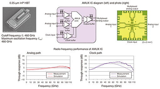
The AMUX and ADEMUX integrated circuits (ICs) for the bandwidth doubler were designed and fabricated using our in-house indium phosphide heterojunction bipolar transistor (InP HBT) [3]. We have already succeeded in conducting a proof-of-principle experiment and beyond-100-GBaud optical transmission [4]. In addition, we recently demonstrated the world’s first 1-Tbit/s-per-channel long-haul WDM (wavelength division multiplexing) optical transmission using 120-GBaud probabilistically shaped PDM 64QAM [5]. These results confirmed that the bandwidth doubler is promising for future beyond-100-GBaud systems. 3. The latest AMUX IC and 160-GBaud signal generationWe are now developing faster AMUX and ADEMUX ICs to further improve optical transmission performance. Using newly developed in-house 0.25-μm InP HBT technology [6], we succeeded in developing an AMUX IC with a bandwidth over 110 GHz (a world record) in 2018 [7]. The performance of the 0.25-μm InP HBTs and AMUX IC is summarized in Fig. 4. The fabricated HBTs have a peak fT (cutoff frequency) and fmax (maximum oscillation frequency) of 460 and 480 GHz, respectively. The AMUX IC consists of two input buffers, a clock buffer, an AMUX core, and an output buffer. It is designed to have broad peaking characteristics in its frequency response to compensate for packaging loss.
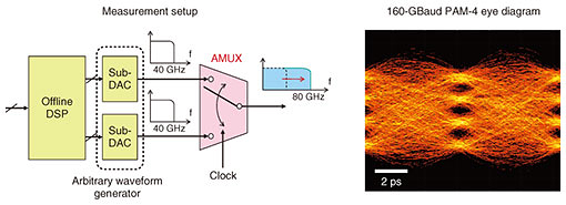
The measured bandwidths for the analog and clock paths were both over 110 GHz. These measurement results indicate that this AMUX IC can potentially be used in constructing a 110-GHz-bandwidth 220-GS/s DAC subsystem and to generate 200-GBaud-class modulated signals. We have already demonstrated signal generation at ultrahigh symbol rates by applying this AMUX IC to the bandwidth doubler. The measurement setup and results are shown in Fig. 5. In this demonstration, we succeeded in generating a 160-GBaud PAM-4 (4-level pulse amplitude modulation) signal with two 40-GHz-bandwidth sub-DACs and the AMUX IC and demonstrating the further scalability of the bandwidth doubler technology [8]. Digital coherent optical transmission with a capacity of over 1-Tbit/s per channel will be achievable by using this AMUX IC.
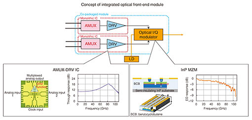
4. Concept of ultrahigh-speed integrated optical front-end moduleOne more important issue for beyond-100-GBaud systems is integration and packaging technology, as mentioned in the first section. This is especially true regarding the transmitter, where the AMUXs, DRVs, and optical modulators have to be placed as close to each other as possible. In addition, all these devices have to be assembled into one integrated packaged module in order to ensure the quality of ultrabroadband modulated signals. We have developed an AMUX IC equipped with a DRV function (AMUX-DRV IC) and studied a design incorporating the AMUX-DRV IC and optical modulators for an ultrahigh-speed integrated optical front-end module. Because monolithic integration of the AMUX function and DRV function into one chip is advantageous for ensuring the signal quality and reducing power consumption, we replaced an output buffer with a DRV function block consisting of a high-gain, high-linearity, and large-output-swing amplifier in the AMUX IC, and designed the AMUX-DRV IC. For the optical front-end, we used in-house InP MZM (Mach-Zehnder modulator)-based optical IQ (in-phase and quadrature) modulators, which have an electro-optical (EO) modulation bandwidth of 80 GHz. The AMUX-DRV IC was designed to have broad peaking characteristics to compensate for the frequency response of the following modulator and to have optimum output impedance and driving voltage for the modulator. A conceptual block diagram of the integrated optical front-end module is shown in Fig. 6, which also summarizes the performance of the AMUX-DRV IC and InP MZM. The AMUX-DRV IC has broad peaking characteristics and ultrabroad bandwidth of over 110 GHz as expected. With this AMUX-DRV IC, the optical front-end module could be expected to have an ultrabroad EO bandwidth of 80 GHz. We have actually already fabricated a sub-assembly that contains the AMUX-DRV IC and InP MZM and have succeeded in demonstrating 400-Gbit/s-per-channel DMT (discrete multi-tone) signal optical transmission [9]. This is a record for IMDD (intensity modulation and direct detection) optical transmission so far and indicates the capability of over-1-Tbit/s-per-channel digital coherent optical transmission. In the next step, we will complete the optical front-end module and apply it to digital coherent optical transmission.
5. SummaryIn this article, we introduced recent trends and challenges in optical communications and our research and development (R&D) of ultrahigh-speed optical front-end device technology for future beyond-100-GBaud systems. We will continue to promote further speed improvements and continue with our R&D so that this technology can ensure sustainable progress of optical communications. References
|
|||||||||||||||||||