|
|||||||||||||||||||||||||||||||
|
|
|||||||||||||||||||||||||||||||
|
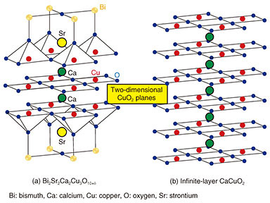
Feature Articles: Creating Novel Functional Materials Vol. 17, No. 10, pp. 18–23, Oct. 2019. https://doi.org/10.53829/ntr201910fa4 MBE Growth and Element-distinctive Atomic-resolution Characterization of High Temperature SuperconductorsAbstractCuprate superconductors are in the material family that have the highest superconducting transition temperature (Tc) of ~130 K under ambient pressure. The infinite-layer structure is the essential building block of high-Tc cuprates with a Tc of over 100 K and is therefore vital to understand the mechanism of high-Tc superconductivity. While the infinite-layer phase is inaccessible using bulk single-crystal synthesis methods, we synthesized single-crystalline thin films of the infinite-layer cuprates using our unique oxide molecular beam epitaxy setup. To clarify the relationship between their microscopic crystal structures and electronic responses, we performed atomic-resolution electron microscopy measurements of the CuO2 (copper peroxide) planes in the infinite-layer cuprates, the playground of high-Tc superconductivity. Keywords: superconductivity, oxide molecular beam epitaxy, scanning transmission electron microscopy  1. IntroductionSuperconductivity is a phenomenon in quantum materials that allows for lossless transportation of electrical current, and thus of energy and information. The quantum phenomenon, superconductivity, had been observed only below –140°C (~130 K) until very recent reports on hydrides, that is, sulfur hydride (H3S) and lanthanum hydride (LaH10). These materials show significantly higher superconducting transition temperatures (Tcs): –70°C (~200 K) for H3S [1] and even close to room temperature for LaH10 [2]. Synthesizing these hydrides, however, requires extremely high pressure, specifically, ~2 million times higher (~200 GPa) than the atmospheric pressure. To make matters more complicated, their crystal structures are altered when the pressure is reduced after synthesis. In other words, the superconducting phases can exist only under an extremely high pressure comparable to that at the core of the Earth. Accordingly, practical applications using these hydrides remain elusive despite the significance of their discoveries from an academic point of view. In contrast, cuprates are superconductors that exhibit the highest Tc under ambient pressure. Among them, YBa2Cu3O7-δ (yttrium barium copper oxide) as well as Bi2Sr2Ca2Cu3O10+δ (bismuth strontium calcium copper oxide), both of which show higher Tc (~90 K and ~110 K, respectively) than the boiling point of nitrogen (77 K), have already yielded practical applications as superconducting cables and microwave filters. However, the mechanism of high-Tc superconductivity in cuprates remains unclarified despite immense efforts for over three decades, which has been hampering the strategic search of novel superconducting materials with a higher Tc. Nonetheless, the fundamental structural ingredient of high-Tc cuprates is fortunately well known: copper peroxide (CuO2) planes, as exemplified by Bi2Sr2Ca2Cu3O10+δ (Fig. 1(a)). Two-dimensional CuO2 planes are made up of copper (Cu) and oxygen (O) and are separated by bismuth (Bi), strontium (Sr), calcium (Ca), and O. The formal valences of O and Cu are 2– and 2+, respectively, so the CuO2 plane is not charge-neutral and cannot exist independently. Instead, the minimal structural unit that is compassable is charge-neutral calcium copper oxide (CaCuO2) (Fig. 1(b)), which is commonly included in cuprates whose Tcs are above 100 K; the crystal structure shown in Fig. 1(b) is called an infinite-layer structure. That is why we have been focusing our research efforts on infinite-layer cuprates. Because the synthesis of bulk specimens of CaCuO2 requires high pressure levels (3–5 GPa), single-crystalline CaCuO2 specimens can be prepared exclusively by using thin-film growth methods, in our case, molecular beam epitaxy (MBE). Unlike the above-mentioned hydrides, the infinite-layer structure is stable at ambient pressure once it is formed.
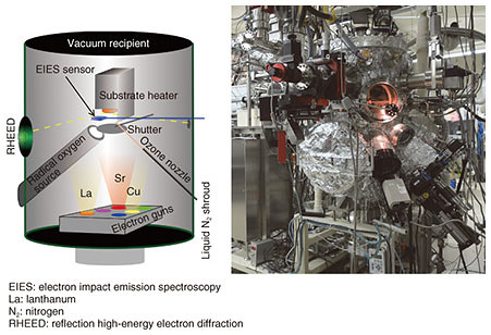
2. Fabrication of ultrahigh-quality infinite-layer cuprate superconductorsWhile MBE has been widely used for the growth of semiconductors, we have extended it to the growth of complex transition metal oxides. Our customized MBE method is well equipped not only to synthesize novel complex transition metal oxides, for example, Sr3OsO6, a new ferromagnetic insulator with a Curie temperature > 1000 K [3], but also to push the limits of common crystal growth methods [4], and this is illustrated in Fig. 2. The vacuum recipient is 70 cm in diameter and 150 cm in height. A total of 10 metal sources are mounted at the bottom of the vacuum recipient where the elements can be evaporated by electron guns operated at 10 kV. The evaporant flux of each element is monitored and controlled by electron impact emission spectroscopy (EIES). The details of EIES are explained in another article in this issue [5].
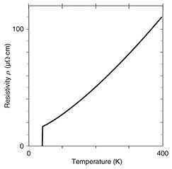
Molecular oxygen (O2) is insufficient for the growth of complex transition metal oxides, and therefore, the oxide MBE system is equipped with stronger oxidizing agents. This is distinct from conventional MBE. In this work, radio-frequency radical oxygen (O) was used for the growth of infinite-layer cuprates. Oxidation/reduction involves the gain/loss of electrons. Radical oxygen has two unpaired electrons and therefore a strong tendency to deprive the neighboring metal atoms of electrons. The absence of kinetic barriers in atomic oxygen is what drives the growth of complex transition metal oxides in an ultrahigh vacuum (~10–9 atm). In addition, the growth orientation is defined by the substrate; this phenomenon is called epitaxy (in Greek, order on top). We used a single-crystal substrate with a lattice constant closer to one for infinite-layer cuprates. This mechanism enables the formation of single-crystalline infinite-layer cuprates. We used the oxide MBE system to synthesize superconducting infinite-layer Sr0.9La0.1CuO2 thin films [6–9]. In Sr0.9La0.1CuO2, strontium ions (Sr2+ ions) are partially substituted with La3+ ions (lanthanum ions) to induce superconductivity. The dependence of resistivity on temperature for the Sr0.9La0.1CuO2 thin film is plotted in Fig. 3. Resistivity decreases as the temperature decreases and abruptly goes to zero at 41 K. The films presented here are superior to those in other reports on superconducting infinite-layer thin films [10], as evidenced by the following characteristics:
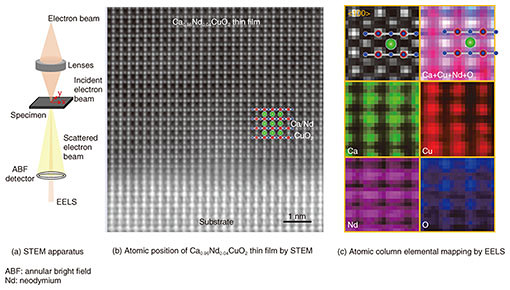
It is therefore shown that samples grown with our method are most suitable to reveal the inherent physical properties leading to understanding the mechanism of high-Tc superconductivity. 3. Infinite-layer CaCuO2—elemental-resolved and atomic-resolution characterizationAs already mentioned, CaCuO2 is an essential structural part of high-Tc cuprates. In contrast to strontium copper oxide (SrCuO2), however, little is known about the physical properties of infinite-layer CaCuO2 due to the difficulty of synthesis. We synthesized infinite-layer Ca1-xNdxCuO2 thin films using MBE. In Ca1-xNdxCuO2, calcium ions (Ca2+ ions) are partially substituted with Nd3+ ions (neodymium ions) by mimicking Sr0.9La0.1CuO2. For a composition of x = 0.06, we found traces of superconductivity around 10 K [11]. It is important to note that a truly superconducting state has not been established. Therefore, it is of significant importance to determine the differences between superconducting Sr1-xLaxCuO2 and non-superconducting Ca1-xNdxCuO2 by using scanning transmission electron microscopy (STEM) combined with electron energy loss spectroscopy (EELS). STEM is used to visualize atomic positions in matter. The configuration of our STEM apparatus is shown in Fig. 4(a) [12]. Accelerated electrons at 200 kV are focused on a sample. The scattered electron beam contains information on the atomic position. This is shown in Fig. 4(b) for Ca0.96Nd0.04CuO2. Because the contrast of the original bright-field image is inverted, the atomic positions appear bright in Fig. 4(b). The observed atomic column arrangements correspond to the infinite-layer structure with two-dimensional CuO2 planes. It is evident that Ca0.96Nd0.04CuO2 thin films are single crystalline. We used EELS to identify the constituent atomic species. This is shown in Fig. 4(c). The atomic selectivity of EELS enables an atomic column identification that exactly matches the infinite-layer phase.
By measuring the distance between Cu and O (dCu-O) from Fig. 4(c), we determined the in-plane lattice constant of Ca0.96Nd0.04CuO2 to be 0.386 nm. This is 0.001 nm longer than for CaCuO2 [13]. Similar expansion is found for the Sr0.9La0.1CuO2 system, where a substitution of 10% of La results in an expansion of 0.002 nm of the in-plane lattice constant [14]. It is intuitively suggested that a critical in-plane lattice constant (dCu-O x 2) for the induction of superconductivity is to be expected. As the ionic size of Ca2+ ions is smaller than that of Sr2+ ions, CaCuO2 has shorter dCu-O than for SrCuO2. During the course of our study, we found that a higher concentration of Nd causes instability of the infinite-layer phase. Consequently, it is not possible to prepare the infinite-layer phase of Ca1-xNdxCuO2 with a sufficient amount of Nd to induce a superconducting transition. This result suggests that lattice constant (the Cu-O bond length in the CuO2 plane) engineering is important for the induction of superconductivity in cuprates. 4. Future outlookInfinite-layer cuprates are very important to understand the physics of high-Tc superconductivity. We plan to apply our thin film growth method to further understand the mechanism of high-Tc superconductivity commonly emerging in materials containing CaCuO2. This method is currently being extended to the synthesis of superlattices containing CaCuO2 [15]. References
|
|||||||||||||||||||||||||||||||