|
|||||||||||||||||
|
|
|||||||||||||||||
|
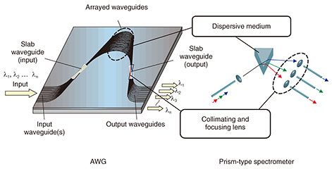
Regular Articles Vol. 19, No. 4, pp. 47–52, Apr. 2021. https://doi.org/10.53829/ntr202104ra1 Progress in Multi-wavelength Receiver Integration with Arrayed Waveguide GratingsAbstractWe describe the progress in integrated wavelength-division multiplexing (WDM) photoreceivers that feature low-loss arrayed waveguide gratings (AWGs) for high-speed throughput of up to 100 Gbit/s and beyond. The design and assembly of optical coupling between higher-order multimode beams and a photodiode are essential to obtain a flat-top spectral shape. We developed 10- and 40-Gbit/s WDM photoreceivers by using mechanical and visual alignment, respectively. We also fabricated a 100-Gbit/s photoreceiver by using high-accurate active alignment. The AWGs and assembly concepts of WDM integration enable scaling up to 400-Gbit/s and beyond and are key to achieving the multi-wavelength All-Photonics Network. Keywords: arrayed waveguide grating, fiber optic communications, planar lightwave circuit  1. IntroductionIn current photonics networks, wavelength-division multiplexing (WDM) is essential for large network capacity. Arrayed waveguide gratings (AWGs) have been globally applied for WDM as wavelength multiplexers and demultiplexers in line with the progress in silica-based planar lightwave circuits (PLCs) [1]. Figure 1 illustrates the configuration of an AWG, which is compared with a conventional prism-type spectrometer. An AWG is composed of input waveguides, an input slab waveguide, arrayed waveguides, an output slab waveguide, and output waveguides. In comparison with a prism-type spectrometer, the arrayed waveguides correspond to a prism as a dispersive medium, and the input/output slabs correspond to collimating and focusing lenses.
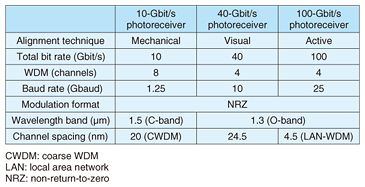
Long-haul traffic has increased owing to the contribution of AWGs in dense-WDM line-side networks. The use of AWGs in shorter reaches is becoming more important because client-side interfaces have also progressed exponentially. Based on current technology trends, client-side networks, such as those used in datacenters and for mobile links with a reach of 100 km or less, will require more data for local wireless traffic with the advanced driver-assistance system, edge computing for artificial intelligence, and automation with Internet of Things. Toward achieving such networks, photonics technology will play a more important role in overcoming electronic limitations on operating frequency and power consumption. In particular, wavelength scalability and functionality through multi-wavelength optical devices will be key to promoting the spread of the innovative All-Photonics Network [2]. We now describe our research and development of WDM photoreceivers integrated with AWGs. Among the various advantages of an AWG, we focus on its low-loss and flat-top functions in a multimode-output AWG (MM-AWG). These photoreceivers are summarized in Table 1. They have different bit rates and are fabricated using several alignment techniques. The 10-Gbit/s photoreceiver was developed using mechanical alignment with eight-channel WDM with a baud rate of 1.25 Gbaud on a 20-nm wavelength grid in the 1.5-μm band. The 40-Gbit/s photoreceiver was fabricated using visual alignment with four-channel WDM with a baud rate of 10 Gbaud on a 24.5-nm wavelength grid in the 1.3-μm band. The 100-Gbit/s photoreceiver was fabricated using active alignment with a baud rate of 25 Gbaud on an 800-GHz or 4.5-nm spectral grid.
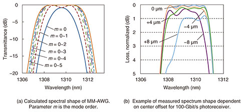
2. MM-AWG and optical couplingInsertion loss and transmission bandwidth are essential parameters in AWG design. Although there are many proposals to improve these characteristics, both are apt to be in a trade-off relationship. We use a special AWG in which multimode waveguides are used at the output slab waveguide. In contrast to the conventional AWG with single-mode output waveguides, the MM-AWG provides a flat-top passband with low loss [3]. Figure 2(a) shows the calculated spectral shape of the MM-AWG. In waveguides, the more the width of the output waveguides is enlarged, the higher the modes are generated, improving spectral flatness together with a reduction in insertion loss. Parameter m is the mode order. In this case, a total of six modes exist including the fundamental one (m = 0). The demultiplexed multimode optical signal is not appropriate for retransmission through a single-mode optical fiber due to the loss of higher modes. Therefore, a photoreceiver in which the multimode signal is instantly converted into electric signal should be used. However, even if the spectral shape is flat at the output of the MM-AWG, poor coupling with a photodiode (PD) degrades the shape. Figure 2(b) shows an example of a measured spectrum dependent on center offset, which is the distance between receiving light axis of the PD and emitting light axis of the PLC. The optical parameters are based on our100-Gbit/s photoreceiver. They show that when the position of the MM-AWG and PD are aligned properly at the displacement of zero micrometers, the flatness of the spectrum is good enough. Therefore, it is important to design optical coupling and consider assembly tolerance to capture all multimode beams to be sufficiently received at the detection area of the PD.
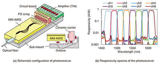
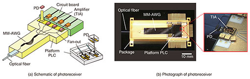
3. Receiver integration using mechanical alignmentThe WDM photoreceiver integrated using mechanical alignment is an eight-channel WDM photoreceiver with a total bit rate of 10 Gbit/s, in which coarse WDM with 20-nm channel spacing and a baud rate of 1.25 Gbaud is applied. A schematic of this photoreceiver is shown in Fig. 3(a). It consists of an MM-AWG, PD array attached to a ceramic carrier, circuit board including transimpedance amplifiers (TIAs), sub-mount, and pigtail fiber, which is connected to the input edge of the MM-AWG. For hybrid integration with the MM-AWG and PD array, we used mechanical alignment. The sub-mount serves as an alignment platform and is made with machining accuracy of better than 10 μm. On the sub-mount shown in the inset, several grooves are formed and filled with bonding adhesive during assembly. This provides high mounting accuracy for the MM-AWG and PD array of better than 5 μm because of the tensile strain induced by the adhesive spreading in the grooves while curing. Therefore, the total placement error in this mechanical alignment is less than 15 μm. The size of the package or sub-mount is 100 × 50 mm. The responsivity spectra of the photoreceiver shown in Fig. 3(b) indicate that a high, flat-top responsivity can be obtained for all channels. Within each passband of 13 nm, the responsivity ranges from 0.7 to 0.85 A/W with a crosstalk level of better than −22 dB. The polarization-dependent loss is 0.2 dB or less at the center wavelength of the grid, which is the same as that of the MM-AWG. We estimated coupling loss between the input fiber and PD as 1 dB, which is the same as in the fiber-coupled measurement; therefore, there is almost no degradation in optical coupling due to mechanical alignment.
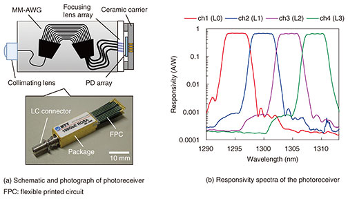
4. Receiver integration using visual alignmentThe second photoreceiver we developed operates at higher speeds and is more compact with 40-Gbit/s throughput. A schematic of this photoreceiver is shown in Fig. 4(a). It is composed of an MM-AWG PLC, platform PLC that integrates fan-out waveguides and PDs, and electrical circuit including TIAs. The PLC of the MM-AWG and platform PLC are bonded in advance with adhesive with high optical transparency. Such a dual-PLC structure can ensure the quality of the two PLCs separately in terms of yield and size. On the platform PLC, edge-illuminated PDs are flip-chip bonded. Visual alignment is used for assembly with higher accuracy than that with the 10-Gbit/s photoreceiver. As shown in the inset illustrating the hybrid integration of the PDs on the platform PLC, alignment is carried out visually using markers on the PD and PLC. The assembly error is less than 1 μm. Designing the fan-out so that the channels are separated can suppress electrical inter-channel crosstalk. According to our estimation from radio-frequency simulation, separation over 1.5 mm provides electrical isolation of more than 20 dB at a frequency of 10 GHz. Figure 4(b) shows photographs of this photoreceiver. The MM-AWG bonded with the platform PLC and circuit board are mounted in a package. The enlarged photograph shows the detecting area, where the PD is hybridly integrated on the platform PLC and connected to a TIA via electrical wire. As we estimated, the measured 3-dB-down bandwidth of the receiver is larger than 9 GHz with an adjacent crosstalk of better than 21 dB. The small and compact package is 64 × 25 mm.
5. Receiver integration using active alignmentThis photoreceiver has a baud rate of 25 Gbaud with throughput of 100 Gbit/s by four-channel WDM. It meets the Institute of Electrical and Electronics Engineers (IEEE)’s standard of Ethernet 100 GbE for transmission reach of 10 and 40 km. A 4-channel WDM with a 25-Gbit/s non-return-to-zero (NRZ) signal and wavelength allocation, called local area network (LAN)-WDM with a grid spacing of 800 GHz [4], is applied. Figure 5(a) illustrates the core assembly of this photoreceiver, which is composed of an MM-AWG, collimating lens, focusing lens array, and PD array, all bonded as a single assembly block. For all the optical connections in the core assembly, we used active alignment in which all the positions of optical components are aligned while monitoring the power of input light. This provides very high accuracy placement by means of inputting an optical signal into each component. A photograph of this photoreceiver is also shown in the figure. The photoreceiver consists of a metal hermetically sealed package, receptacle Lucent (LC) connector with another focusing lens, and flexible printed circuits. The size of the package is 7 × 18 × 6 mm3, which can be installed in compact Ethernet transceivers. Figure 5(b) shows the responsivity spectrum of the photoreceiver. We observed a flat-top spectral shape of over 500 GHz and a maximum responsivity higher than 0.7 A/W for all channels. The total optical loss is about 1.5 dB, which includes 0.8-dB AWG loss, 0.3-dB coupling loss from the PLC to PD, and 0.3-dB loss from the PLC to receptacle. The crosstalk between adjacent channels is less than 25 dB in the 360-GHz passband. We also conducted reliability tests, such as temperature tracking from 5 to 80°C, high-temperature storage at 85°C, and mechanical vibration. In all tests, a loss change as low as less than 0.2 dB was confirmed, which reveals the high reliability of the photoreceiver owing to our stable assembly. For the bit-error-rate (BER) characteristics, we obtained a minimum receiver sensitivity of less than −10.9 dBm in optical modulation amplitude (OMA) at a BER = 10−12. These results meet the specifications for 10-km 100 GbE links with a sensitivity margin of over 4 dB. By replacing the pin-PD with an avalanche PD, we confirmed further extended reach of 40 km [5].
6. Further studiesWe have used the MM-AWGs and assembly concepts described in this article toward beyond-100-Gbit/s applications such as for ramping up to 200-Gbit/s throughput by adopting four-level pulse-amplitude modulation (PAM4) and 400-Gbit/s photoreceiver using an eight-channel WDM together with the PAM4 format [6–8]. These consecutive studies have clearly shown our receiver integration technology is promising for future client-side communications as well as the All-Photonics Network. References
|
|||||||||||||||||