|
|||||||||
|
|
|||||||||
|
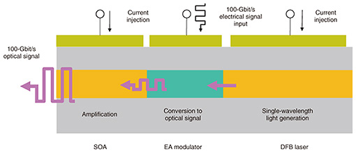
Feature Articles: Device Technologies for Enabling the All-Photonics Network Vol. 20, No. 8, pp. 15–21, Aug. 2022. https://doi.org/10.53829/ntr202208fa1 High-output Optical Transmitter and High-sensitivity Optical Receiver for 400-Gbit/s 40-km Fiber-amplifier-less TransmissionAbstractWe developed a high-output optical transmitter and a high-sensitivity optical receiver for long-distance transmission in the All-Photonics Network that is being promoted under IOWN (the Innovative Optical and Wireless Network). This article introduces the 400-Gbit/s optical transmitter with a semiconductor optical amplifier-assisted extended-reach electro-absorption modulator integrated distributed feedback laser called AXEL, a key device for higher optical output, and the 400-Gbit/s optical receiver with an avalanche photodiode, a key device for higher sensitivity. Keywords: intensity-modulation direct-detection (IM-DD), AXEL, APD  1. IntroductionThe amount of data handled by communication networks has been increasing dramatically with the development of cloud services and other new services, and traffic volume has also been increasing sharply. In response, NTT proposed the Innovative Optical and Wireless Network (IOWN) to increase transmission capacity, decrease latency, reduce power consumption, and provide excellent flexibility in the communication network. The All-Photonics Network (APN), one of the three main components of IOWN, will introduce photonics technology everywhere, from the network to the terminal and from short distances to long distances, to achieve overwhelmingly lower power consumption, higher quality, greater capacity, and lower latency in network-data transmission. At the NTT Device Innovation Center, we developed an optical transmitter and optical receiver for intensity modulation format to fabricate a compact and low-power-consumption transceiver and increase transmission capacity. To fabricate the transmitter and receiver for long-distance transmission, a higher output optical transmitter and higher sensitivity optical receiver are needed. We therefore conducted research and development on a semiconductor optical amplifier (SOA)-assisted, extended-reach electro-absorption modulator integrated distributed feedback (EADFB) laser called AXEL [1], which is a key device for high optical output, and an avalanche photodiode (APD) [2], which is a key device for high sensitivity. This work resulted in the development of an optical transmitter and receiver that are capable of transmitting a 400-Gbit/s signal over a distance of 40 km [3, 4]. The developed transmitter and receiver extend the region in which intensity modulation can be applied, contributing to reducing network-interface device size and power consumption. 2. AXELThe key device of the high-output optical transmitter is a high-speed, high-output optical transmission device, which is generally an EADFB laser that generates an optical signal of 100 Gbit/s per chip. This laser comprises a DFB laser that emits single-wavelength light and an EA modulator that converts an electrical signal to a high-speed, high-quality optical signal. However, conventional EADFB lasers have high optical loss in the EA modulator and inhibit the increase in higher output power. To address this issue, we have been developing AXEL as a key transmitter that can achieve high-speed optical transmission with high output (Fig. 1). An SOA is driven by current injection, and light incident to the SOA is amplified as it propagates. In conventional EADFB lasers, the intensity of the light output by the DFB laser is decreased by modulation in the EA modulator, but in AXEL, the light is amplified by the SOA to obtain a high-output optical signal. The SOA is fabricated from the same semiconductor materials as the DFB laser; therefore small, integrated AXEL chips can be fabricated with the same process, enabling low-cost mass production. Because each SOA chip must amplify a high-speed 100-Gbit/s optical signal, this SOA uses a new optical amplification layer that efficiently converts electrical current into light with less degradation in the optical waveform, thus achieving output of a 100-Gbit/s signal with no loss of quality. The AXEL chip we developed is thus capable of outputting a 100-Gbit/s optical signal with an intensity of +8.0 dBm or more [1]. An optical transmitter that generates a 400-Gbit/s optical signal can be achieved with an array of four discrete AXEL chips.
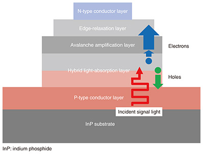
3. APDThe key device of the high-sensitivity photoreceiver is a high-speed, high-sensitivity PD. The PDs that are generally used in receivers have a theoretical opto-electrical conversion efficiency of 100%, but, in most cases, the actual efficiency is only a few tens of percent because of loss at light incidence and incomplete absorbance of light within the PD. We developed an APD, a special PD designed to serve as a high-speed, high-sensitivity receiver. A strong electric field is induced within the APD, and more electrons and holes are generated by collisions of ionized photoelectrons in the field. The result is an opto-electrical conversion efficiency that can exceed 100%, enabling the fabrication of a high-sensitivity optical receiver. The main components of the APD are light-absorption layers and an avalanche amplification layer (Fig. 2). The optical signal is converted to an electrical signal in the absorption layers, and the resulting electrical signal is amplified in the amplification layer.
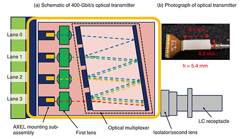
The APD converts a 100-Gbit/s optical signal to an electrical signal. PDs generally must sacrifice sensitivity to received light to achieve higher speed. They also require a waveguide that makes photonic coupling of the incident optical signal to them difficult. For this APD, we adopted a hybrid two-layer light-absorption structure that combines one absorption layer that uses electron diffusion as the main carrier-transport mechanism and another absorption layer that uses hole drift as the main carrier-diffusion mechanism. This makes it possible for the optical receiver to handle a 100-Gbit/s signal while maintaining high sensitivity and facilitating optical coupling with a vertical injection structure [2]. An optical receiver that converts a 400-Gbit/s optical signal to an electrical signal can be fabricated by mounting four APD chips. 4. 400-Gbit/s high-output optical transmitterOur four-channel, 400-Gbit/s optical transmitter achieves high output power with four AXEL chips that are mounted inside the transmitter on four sub-assemblies (Fig. 3(a)) [3]. Each chip outputs a 100-Gbit/s optical signal. The light wavelengths output from the subassemblies, 1295.5 nm (Lane 0), 1300 nm (Lane 1), 1304.5 nm (Lane 2), and 1309.1 nm (Lane 3), are determined using a local area network-wavelength division multiplexing grid. The output light is collimated after passing through the first lens and input to an optical multiplexer that comprises a mirror, glass block, and wavelength filters. The 400-Gbit/s optical signal from the multiplexer is passed through an isolator and the second lens and then coupled to an internal optical waveguide in a Lucent connector (LC) receptacle. A photograph of the fabricated compact 4-channel optical transmitter is shown in Fig. 3(b). The device is 18.2 mm long, 6.2 mm wide, and 5.4 mm high, small enough to be mounted in a quad small-form-factor pluggable, double density (QSFP-DD) optical transceiver.
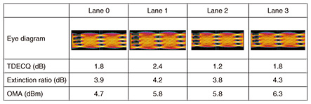
We measured the waveform eye diagrams and the output power for operation at 400 Gbit/s. The AXEL chip temperature was 50°C. The laser diode and SOA currents were 80 and 40 mA, respectively. The measured electrical signal was 53.125 Gbaud, and the amplitude voltage of the four-level pulse amplitude modulation signal was 0.75 Vpp. The eye diagrams were observed with a sampling oscilloscope after the signal was passed through a 26.6-GHz low-pass filter and equalization with a transmitter dispersion eye closure quaternary (TDECQ) filter. Clear eye openings were obtained for all lanes, with TDECQ (an indicator of waveform quality) of 2.4 dB or less (Fig. 4). Optical output power (optical modulation amplitude (OMA)) of at least +4.7 dBm was also confirmed for all lanes, indicating the high output characteristic of the AXEL chip.
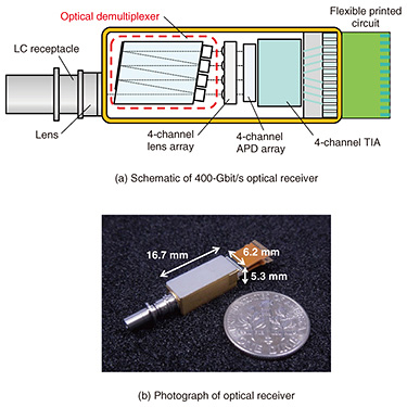
5. 400-Gbit/s high-sensitivity optical receiverThe optical receiver comprises a collimating lens for the light output from the LC receptacle, optical demultiplexer for demultiplexing the four-wavelength optical signal from the transmitter, four-channel lens array, four-channel APD array, and four-channel trans-impedance amplifier (TIA). The optical signal input to the receiver is separated into wavelengths of 1295.5, 1300, 1304.5, and 1309.1 nm by the optical demultiplexer (Fig. 5(a)) [4]. The demultiplexed optical signals pass through the lens array and input to the four-channel APD array for conversion to amplified electrical signals. The four 100-Gbit/s electrical signals are output from the receiver via the TIA. A photograph of the fabricated four-channel optical receiver is shown in Fig. 5(b). The device is 16.7 mm long, 6.2 mm wide, and 5.3 mm high, small enough to be mounted in a QSFP-DD optical transceiver in the same manner as the transmitter described above.
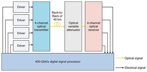
We measured the bit-error-rate (BER) of the fabricated four-channel optical receiver with the system configuration illustrated in Fig. 6. The four-channel optical transmitter outputs one 100-Gbit/s signal per channel to generate a total signal-transmission rate of 400 Gbit/s. The extinction ratio for the optical signal ranges from 3.8 to 4.3 dB. The signal is input to the four-channel receiver via the variable attenuator, converted to an electrical signal, then output. The output signal is demodulated by the 400-Gbit/s digital signal processor and the BER is calculated under discrete operation.
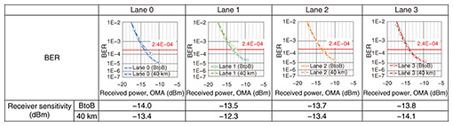
The BER for each channel is shown in Fig. 7. In a back-to-back (BtoB) configuration, where the optical transmitter and optical receiver are connected almost directly, the minimum receiving sensitivity for a BER of 2.4 × 10⁻⁴ ranged from –13.5 to –14.0 dBm for OMA. When the receiver was connected to a 40-km standard single-mode fiber as a transmission line, the minimum receiving sensitivity for OMA ranged from –12.3 to –14.1 dBm. These results indicate that the transmission distance in a 400-Gbit/s transmission service can be extended to 40 km by combining a four-channel optical transmitter assembled with AXEL chips and a four-channel optical receiver assembled with APD chips and using intensity modulation.
6. ConclusionWe fabricated a compact high-output four-channel AXEL transmitter and compact high-sensitivity four-channel APD receiver for 400-Gbit/s application. The transmitter and receiver are capable of transmitting a 400-Gbit/s optical signal to a distance of 40 km over optical fiber by intensity modulation, with the expectation of a reduction in power consumption. These indicate that the fabricated AXEL transmitter and APD receiver are promising technology for high-capacity and energy-efficient networks. References
|
|||||||||