 |
|||||||||||||||||
|
|
|||||||||||||||||
|
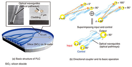
Feature Articles: Optical Device Technologies for Next-generation Computing Using Light Vol. 20, No. 8, pp. 52–57, Aug. 2022. https://doi.org/10.53829/ntr202208fa7 Optical Circuit Technologies for Next-generation Computing Using LightAbstractTo sustainably achieve a society in which digital technologies have penetrated in various forms such as smartphones and cloud services, computing technologies that greatly exceed the current performances are becoming important. NTT is advancing research and development of computing technology using lightwaves/photons by applying device technology for communications using optical waveguides. In this article, we introduce optical circuit technology mainly for optical quantum computing as an example. Keywords: optical circuits, planar lightwave circuits, optical quantum computers 1. Optical circuit technology for computing using lightwavesA variety of optical devices have been developed for optical fiber communications by using planar lightwave circuit (PLC)* technology (Fig. 1(a)), in which the circuit is fabricated by combining optical fiber and semiconductor manufacturing technologies [1]. PLC technology is considered a promising device technology for computing using light as an optical circuit technology capable of integrating linear optical elements.
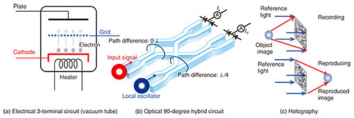
Electronic devices, such as transistors, three-pole vacuum tubes, and three-terminal regulators, can be classified as three-terminal devices. They have inputs and outputs, and the desired output can be obtained by reflecting the control signals from the control terminals to the input state. A computer is composed of a very large number of transistors, which are three-terminal devices. In a vacuum tube (Fig. 2(a)), for example, the operation of the three-terminal device is controlled by the voltage applied to the intermediate terminal called the grid. Regarding optical devices, there are optical switches and optical modulators that drive control terminals from electronic devices, but from the viewpoint of computing using light, the input to the control terminals must also be light. One such device that can be considered a three-terminal device is an optical interferometer. An optical interferometer outputs the interference light from multiple optical inputs. It is considered a three-terminal device by regarding some of the optical inputs as ports of light for control. Figure 1(b) shows the basic operation of a directional coupler, a type of interferometer often used in PLC technology. When two optical waveguides (paths of light) are brought close together, light is transferred from one optical waveguide to the other. By separating the optical waveguide at half the length of the complete transition, we can split the input light into two lights with phase difference by π/2. The input from the other optical waveguide is also divided into two lights with the phase difference of π/2. When these are input and superposed at the same time, and one is considered an input port and the other a control port, and if the output from the two waveguides on the output side is considered one output state, it becomes a three-terminal optical circuit that controls light by the phase difference between the light at the input and control ports. An example of a device using this interferometer is an optical circuit called an optical 90-degree hybrid circuit [1] (Fig. 2(b)), which can measure both the phase difference and amplitude of the input signal with respect to the local oscillator light (local coherent light) used in coherent transmission. In coherent transmission, local oscillator light with a constant frequency is used. In optical quantum information processing, which is introduced later, local oscillator light is combined with the entangled state as a control signal to enable quantum teleportation to obtain a desired output. For another example, the holographic recording process can be regarded as a three-terminal device for obtaining a Fourier transform image if the image light is used as an input and the reference light is regarded as a control light (Fig. 2(c)).
If an optical circuit in which multiple inputs interfere with each other can be regarded as a three-terminal device, it is expected to enable new information processing using light, similar to processing by a computer composed of vacuum tubes and transistors. Quantum information processing using optical circuits is introduced as a concrete example.
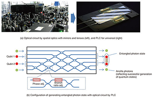
2. Quantum information processing using optical circuitsQuantum computers use superposition and entanglement of quantum states to solve problems that cannot be solved using a conventional computer in practical terms. Various physical quantum states and their implementations have been proposed for use in quantum computers, including superconducting circuits and ion traps. Optical quantum computers using photons are promising candidates of feasible quantum computers because they can operate at room temperature and at high speed. Optical quantum information processing using optical circuits is mainly divided into two types, mode (or path qubit) and continuous-variable, which are introduced below. 2.1 Mode-type optical quantum information processingMode-type optical quantum information processing uses photon states (mode) in optical waveguides. There are two methods of expressing a qubit. One provides a qubit as superposition of a state with and without a photon in one optical waveguide (single-rail representation), and the other expresses a qubit by superposition of a state with a photon in either waveguide using two optical waveguides (dual-rail representation). To achieve the nonlinear operation required for quantum information processing in a linear circuit, it is necessary to achieve it stochastically in combination with measurement. In the single-rail representation, it is difficult to distinguish whether a photon has disappeared due to loss or a change in the quantum state. However, the dual-rail representation always manipulates the state in which a photon is present, so it is easy to detect whether a quantum operation has succeeded by combining it with an auxiliary photon (ancilla photon). Using dual-rail representation and posterior selective processing of successful quantum states, research is being conducted to achieve larger-scale quantum computing. NTT has fabricated the world’s first 6 × 6 universal quantum optical circuit using PLC technology (Fig. 3(a)). Conventionally, it had difficult to ensure stability because of the extremely large size of the optical system constructed with spatial optics on an optical bench. However, by making it a chip, a compact and stable optical system was achieved. The configuration of the optical circuit is shown in Fig. 3(b). The part where the optical waveguides appear to intersect is equipped with a heater that locally changes the refractive index by the thermo-optic effect, and the phase and branching ratio can be adjusted. Although it may look like a complex circuit, it combines the basic operations of interfering photons in a directional coupler, allowing variable, arbitrary linear operation (6 × 6 unitary operation). In collaboration with the University of Bristol, we have confirmed that various types of quantum information processing can be executed with high precision [2]. Figure 3(b) shows the configuration of an optical circuit that generates an entangled state from two qubits in a dual-rail representation. To implement a practically useful quantum computer, it is necessary to further increase the scale, but in addition to increasing the number of waveguides, it is also necessary to develop a more advanced circuit configuration, such as post-selecting only successful quantum states reflecting the states of ancilla photons and transmitting them to the subsequent stages.
2.2 Continuous-variable-type optical quantum information processingA quantum computer using a continuous variable system has also been proposed. With a continuous variable system, the quantum state is determined by measuring the interference state with the reference light by putting information on the phase and amplitude of the lightwave as in the case of radio or optical fiber communications. This is called projection measurement because the base of the state to be measured can be specified by changing the way the reference-light state interferes with the observed state. For example, a 90-degree hybrid circuit, as a measurement of the classical state, is, from a quantum mechanical point of view, a projective measurement (bell measurement) that detects photons in the mode corresponding to the entangled state (bell basis) of the input and reference light. By using the result of the bell measurement of one of the entangled states, quantum teleportation can be achieved by phase-shifting another one of the entangled states (Fig. 4(a)). This circuit is extremely important as a basic operation of measurement-type quantum computation, which executes quantum information processing by measurement with feedforwarding via a classical path. In cooperation with the University of Tokyo, we fabricated a PLC circuit that operates in the 850-nm band, as shown in Fig. 4(b). As a preliminary study, we evaluated the squeezed light output from the circuit and confirmed a squeezing level of approximately 3.2 dB, which enables non-classical operation [3, 4]. To achieve a level sufficient for quantum computation, including quantum teleportation, we are now shifting to research on quantum information processing in the 1.5-μm band, where device technology for telecommunications can be widely applied, and are vigorously improving the characteristics, such as transmittance of optical circuits.
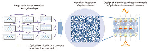
3. Future technology of optical circuit technology for computation using lightAs we have seen, multiple inputs interfere with each other in a way that corresponds to a three-terminal element in an electronic circuit, enabling new information processing with light. In addition to the research introduced in this article, research on neural networks using optical circuits has been vigorously studied. However, how to scale a computational circuit using light is a major issue for its practical use as a computing technology in the future. When optical chips are connected and scaled, as with electronic devices, optical interference is lost or delayed when data transmission is converted to digital data. Even when optical chips are connected with optical fibers, loss and phase shift become unavoidable (Fig. 5, left). Therefore, we need a different approach than combining elements such as electronic circuits and scaling them up. One method is to use the time domain to compute by using the entanglement/correlation between light pulses. Examples using the time domain include continuous quantum optical information processing using multiple pulses described in this article and optical reservoir computing introduced in the article “Photonic Implementation of Reservoir Computing” [5] in this issue. Another means of scaling up is to increase the spatial density. As long as optical interference is used, the size of the components of the optical circuit is limited to the size of the wavelength of light. However, in mode-type optical quantum information processing, for example, a method using multi-value states (qudits) with multiple waveguide modes instead of binary (qubit) states has been proposed. As an extreme case of infinitely increasing the number of modes on the basis of this idea, we can use an approach called monolithic integration of optical circuits, in which information is carried on the wavefront instead of the mode, and computing is executed by interference. The wavefront-matching method has been proposed as an optical-circuit design method that uses the entire refractive index distribution of an optical circuit, and it has been shown that the optical circuit corresponds to a neural network when the entire refractive-index distribution is considered an optical circuit [6] (Fig. 5, right). A neural network based on the evolution equation of the Schrödinger network [7] has also been proposed.
It is expected that optical circuit technology, which enables computing using light, will continue to be developed toward the next generation of computing technology in conjunction with the development of new technologies such as optical quantum computers and neural networks. References
|
|||||||||||||||||

