|
|
|
|
|
|
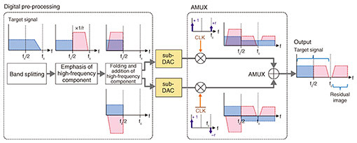
Rising Researchers Vol. 20, No. 8, pp. 11–14, Aug. 2022. https://doi.org/10.53829/ntr202208ri1  Bandwidth-doubler Technology Eliminates Bandwidth BottlenecksAbstractIn communication systems that involve signal processing using digital circuits, the bandwidth at the interface between digital and analogue is a bottleneck to improving communication speed. We spoke to Distinguished Researcher Hiroshi Yamazaki, who developed the principles of the bandwidth-doubler technology for solving this bottleneck. Keywords: bandwidth doubler, digital signal processor, analogue multiplexer  Bandwidth-doubler technology for doubling optical communication speed—What are the ways to increase speed in optical communication? The speed at which information is transmitted in communication is determined by the product of spectral efficiency and bandwidth. Spectral efficiency refers to the amount of information that can be transmitted per unit frequency and time. For example, compared with a binary system that represents “0” when the light is off and “1” when the light is on, a quaternary system that represents four values “00,” “01,” “10,” and “11” with four different states of light can transmit information twice as efficiently. Spectral efficiency in optical communication has been dramatically improved in recent years due to performance improvement in digital signal processors (DSPs) and the evolution of algorithms. Meanwhile, bandwidth refers to the range of available frequencies. The pace of bandwidth expansion, however, has been relatively slow. A particular challenge lies in the analogue bandwidth of the digital-to-analogue converter (DAC) and analogue-to-digital converter (ADC), which convert digital and analogue signals at the input/output unit of the DSP. The DAC and ADC are monolithically integrated with the DSP using complementary metal oxide semiconductor (CMOS) technology. However, while CMOS is almost the only technology in the construction of large-scale digital circuits, it is not necessarily the best technology from an analogue bandwidth perspective. As a result, the bandwidth limitations of DACs and ADCs formed using CMOS technology are becoming a bottleneck in the bandwidth for the entire communication system. Bandwidth-doubler technology can be used to eliminate this bandwidth bottleneck in order to increase the transmission capacity per transceiver. —What is the principle of the bandwidth-doubler technology? Figure 1 shows the principle of the bandwidth-doubler technology. Two DACs (sub-DACs) are arranged in parallel, and their outputs are multiplexed with an analogue multiplexer (AMUX) to transmit a signal with twice the bandwidth of the signal output by each sub-DAC. Currently, we are focusing mainly on the DAC side (transmitter side), so I will focus my explanation on that.
In the middle of the diagram, the yellow section with two sub-DACs is the bottleneck area. The figure shows many light blue and pink graphs on the right and left of the bottleneck. The “f” on the horizontal axis of the graphs refers to frequency, wherein a wide bandwidth means a wide range extending along the horizontal axis, and a narrow bandwidth means a narrow range along the horizontal axis. The “target signal” on the left-hand side of the figure is the signal you want to output and has a bandwidth of fc. However, the sub-DAC only has a bandwidth of fc/2, i.e., half of fc. In other words, the entire signal cannot be transmitted in its original state, but the signal must not be partly cut off. Therefore, it is necessary to think about how to send the entire target signal through the sub-DAC. In the bandwidth-doubler technology, digital pre-processing is first carried out in the DSP, where the target signal is separated into low and high frequencies at fc/2 as the threshold. The high-frequency components are then emphasized; these are the pink parts. Two signals are then created, namely, signals with positively and negatively folded high-frequency components. Since these signals have a width of only fc/2, they can pass through the sub-DACs. The signals then enter the AMUX. The AMUX is a simple electronic circuit in which two input signals are alternately connected to an output at high speed, without distorting the waveform. Switching at a fixed timing is equivalent to making a copy of the input signal (called an image) around the switching frequency fc on the frequency axis. This widens the bandwidth of the signal. Further, by combining the positive and negative relationship of the above two signals with the positive and negative relationship of the image, the light-blue-colored low-frequency component and the pink-colored high-frequency component reinforce each other in the original frequency domain and cancel each other out in the rest of the frequency domain. This enables the target signal to eventually be transmitted. The method shown in the figure is the initial version, and we have now validated a method that enables the clock frequency to be halved. —How is the progress of the research? Bandwidth-doubler technology was first applied to a relatively simple short-range intensity-modulation direct detection (IMDD) transmission system, where it broke the world record in IMDD optical transmission capacity at 250 Gbit/s per wavelength at that time (2016). Since then, we have widened the device’s bandwidth and improved the folding method, increasing the capacity to 400 Gbit/s per wavelength. Also, experiments are underway for digital coherent transmission systems for medium- to long-range applications, and long-distance transmission of high-capacity signals over 1 Tbit/s per wavelength has also been achieved. These results have been published and gained wide attention as top-scoring papers and post-deadline papers by the Optical Fiber Communication Conference (OFC) and the European Conference on Optical Communication (ECOC), the most prestigious academic societies in the field of optical communication. Various approaches have been proposed in attempts to increase capacity, including by other companies and other organizations. We are also in the midst of competition among the top players.
Investigation of improvements in both device technology and signal processing—What are the future prospects? Bandwidth-doubler technology is basically intended for application in optical communication systems. The demand for larger capacities for the devices that make up the optical fiber communication system, especially optical transceivers, is expected to continue in the future. Therefore, we will continue to work on bandwidth expansion technology as one of the approaches to meet these demands. One of our missions is to deploy and promote the innovation of scientifically and academically superior, world-leading technologies, so we will continue our research in this area. From a technical perspective, there is still room for improvement in the bandwidth doubler, so we are pursuing research both from the device technology and signal processing aspects. For example, developing an implementation technology for compact integration of AMUX and optical modulators is one of the important issues to address. Furthermore, since the idea of bandwidth expansion is not tied to a specific device configuration, we will also aim to develop technologies that enable optical circuits to achieve the same functions as AMUX. —What led you to the bandwidth-doubler principle? There were various hints that led to conceiving the bandwidth-doubler principle. I had been conducting research primarily on optical devices until around 2015. In a world where all optical devices were analogue, increasing the capacity of communication entailed various problems. I had also been studying about digital and other technologies, and it was around the time I realized that the improvements in communication capacity in the analogue world would soon reach their limits and high-speed AMUX technology was developed, which led to the idea of the bandwidth doubler, where analogue and digital work together to expand bandwidth. Although at that time the digital part was outside my specialization, it helped that the environment was in place for easily carrying out various experiments. —Could you give a message to students, young researchers, and future business partners? When I talk to researchers from other companies or other institutions at academic conferences, I hear about their problems, e.g., that although they were able to fabricate the device, it is difficult for them to conduct system experiments, and that they do not have access to the devices they want to use for system experiments. NTT has laboratories that are conducting research across a wide range of fields from devices to systems and that are collaborating in various ways. I think this is a major advantage for us. I am a member of both NTT Device Technology Laboratories and NTT Network Innovation Laboratories. And various achievements have come about, including the bandwidth-doubler technology described above, in collaborations between the two laboratories and with the NTT Device Innovation Center. I would like to say to students and young researchers that having a different combination of “drawers” from those of other people is an advantage. As a device researcher, I also learned about digital signal processing, which is not my specialization, leading to the development of the bandwidth-doubler technology. Please do not hesitate simply because it is outside your specialization or because you are a beginner, if it is necessary, take the bold step to learn about the knowledge and technologies in other fields. ■Interviewee profileHiroshi Yamazaki joined Nippon Telegraph and Telephone Corporation in 2005 as a member of NTT Photonics Laboratories. He is engaged in research and development of integrated photonic devices. Currently, he holds concurrent research positions at NTT Device Technology Laboratories and NTT Network Innovation Laboratories. He has a Doctor in Engineering, and is currently the Deputy Editor of Journal of Lightwave Technology. |