|
|
|
|
|
|
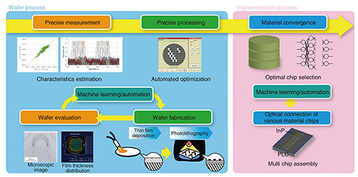
Rising Researchers Vol. 20, No. 9, pp. 12–15, Sept. 2022. https://doi.org/10.53829/ntr202209ri1  Smartphotonics® for High-performance Optical Functional Devices That Are Essential for the Future of IOWNAbstractOptical functional devices are becoming increasingly widely used and important. There is a need, however, to improve not only their functions and performance, but also development time and manufacturing throughput in order to meet the sophisticated and diverse demand specifications. We interviewed Distinguished Researcher Dr. Kenya Suzuki about smartphotonics® to address these problems in the manufacture of optical devices. Keywords: smartphotonics®, process feed-forward method, optical device  Smartphotonics® to manufacture optical functional devices—Tell us about smartphotonics®. Optical device technology is important in a wide range of areas, including optical communications and optical sensing, such as for the Innovative Optical and Wireless Network (IOWN) All-Photonics Network (APN). There are challenges, however, in terms of performance limitations and manufacturability in their design and manufacturing processes. Smartphotonics® is defined as a technical approach to optimize research and development (R&D) and improve manufacturing through automation and statistical prediction to facilitate the fabrication of high-precision optical functional devices (Fig. 1).
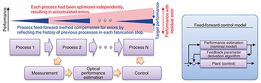
Conventionally, errors in the manufacturing processes for optical devices have been manually corrected, but many problems from human errors occur due to the dependence on individual skills. We started research on smartphotonics® for the automation and consistent production of high-performance optical devices. To explain using architecture as an example, in constructing buildings, tolerance levels are defined for the accuracy of cutting wood and other processes. Any deviation within a certain range is acceptable in constructing a building without any gaps. In general, a building is completed after going through many processes. If tolerance levels are defined for each of those processes, there would be a need to ultimately allow a very large tolerance level. One of the goals of smartphotonics® is to extremely minimize the tolerance levels and deviations in each process in order to improve the performance of the final product. In other words, research on smartphotonics® is aimed at making sure that we can achieve the desired performance by correcting errors in the previous process at every manufacturing step to eventually achieve stable quality. This may be similar in principle to the smart factory. For example, the issue of automation is a commonly recognized problem, and research is being conducted mainly focusing on achieving smart operations by leveraging the characteristics of optical devices. The Optical Switch Module Project, where I serve as the project leader, is developing a device called a multicast switch. This is the key device used for routing and switching optical paths to provide an alternative route to ensure communications, for example, in the event of an earthquake or disaster that causes the optical fibers to fail. This switch is fabricated by repurposing the manufacturing technology for the so-called LSIs (large scale integrated circuits), such as central processing units and memory. My group is developing a multicast switch using silica-based planar lightwave circuit (PLC) that uses the same glass material as optical fibers to create an integrated optical circuit on a wafer. Research on smartphotonics® was started as research on fundamental technologies for creating such devices with high performance. The motivation for this research is to manufacture high-performance optical functional devices required by the APN. We also want to reduce device reworks that occur due to various errors in the manufacturing of optical devices. We believe that smartphotonics® technology will enable the stable and high-volume manufacture of optical functional devices, even in the future when demand for such devices grows due to diversification of applications, such as when optical functional devices come into widespread use in ordinary households. —How do you specifically manufacture with smartphotonics® technology? We have proposed a process feed-forward method as the key to the implementation of smartphotonics® technology. The process feed-forward method is based on the idea of creating high-performance optical functional devices by reflecting the error information generated in the manufacturing process into later processes and sequentially compensating for the errors in each process. Although optical device wafers are manufactured through various processes, they are not optimized at each process as described above, but the different processes are coordinated so that they can produce a good product as a whole. In addition to wafer processing, we are also considering its use in developing devices that combine different materials such as silica-based PLCs and optical semiconductors. While it is normal to yield good performance when you combine products with good performance results, our goal is to create high-performance devices that maximize performance to achieve the target values, even when combining products of moderate performance. Figure 2 illustrates the process feed-forward method in the manufacturing process of optical functional devices. In optical integrated circuits using wafers as substrates, the index of refraction has a large effect on the optical characteristics of devices. This refractive index value can vary every time the device is manufactured, which causes a major problem. To address this problem, first, we precisely measure the refractive index and thickness of glass and then use statistical techniques to estimate the performance as an optical device. When discrepancy and error are likely to occur, we change the thickness, etc. of the core part that propagates light in the next step and optimize the process so that the equivalent refractive index is the same. Unlike in conventional processes where errors would accumulate and performance would widely vary, the process feed-forward method enables the stable manufacture of high-performance devices with minimal performance variations through repetition of these corrective steps in each process.
Realizing the IOWN concept by creating high-performance optical functional devices—What are the future prospects for applications of smartphotonics®? We have just started our research on smartphotonics®. To eventually realize the IOWN concept using this technology, we are aiming to further develop and deploy various devices for wide use. Currently, we are mainly applying smartphotonics® to silica-based PLC technology. We intend to apply the ideas and essence of the technology polished through this application to optical semiconductors and optical devices based on other materials in order to ensure good performance. Smartphotonics® could be a fundamental technology that underpins research on various optical devices. The field of optical devices has thus far been highly specialized for each material and conversations among engineers beyond their expertise have not always been easy. We want to expand the applications of smartphotonics® across a variety of disciplines and enable sharing of the essence of each area of expertise. One of our goals is to create an unprecedented integrated device that combines the best of each material by deploying smartphotonics® technology in all devices. The manufacturing of optical devices also has its own unique properties; some devices are being manufactured using equipment with a slightly older design. For areas where old and difficult-to-replace equipment is still used, we believe that smartphotonics® can be applied to the automation technology for the control of those equipment. The digital transformation market is estimated to reach several hundred billions of yen by 2030. We believe that some of the technologies we have developed in our research can be deployed to a wide range of manufacturing areas where these old equipment remain, such as small businesses and local factories. They can be used as background technologies for automation and the shift to Internet of things.
—Could you give a message to researchers, students, and business partners? I currently belong to the NTT Device Innovation Center, which I think provides one of the best R&D environments in Japan. In particular, we have access to a wide range of hardware research facilities. I think the NTT’s R&D environment, which enables you to test and realize your ideas, is ideal for those who enjoy doing research and are fond of creating new things or taking on different challenges. Although writing papers is also a part of our activities, the NTT Device Innovation Center is an organization aimed at the practical use of devices, so you are expected to conduct development of devices that give users a value and can actually be used. This entails constantly having conversation with users and identifying their issues, as well as creating industry trends. Because the optical device industry has a global market, meetings with foreign counterparts occupies a great part of our daily activities. In this sense, R&D of devices is characterized by a different kind of rigor from writing papers, but it is interesting to see the techniques and methods you propose become trends in the real world. This is a message to young researchers and students. Going forward, through R&D, I will work with researchers, students, and business partners to create value that is recognized not only in Japan but also around the world. ■Interviewee profileKenya Suzuki received a B.E. and M.E. in electrical engineering and Dr. Eng. in electronics engineering from the University of Tokyo in 1995, 1997, and 2000. In 2000, he joined NTT. From September 2004 to September 2005, he was a visiting scientist with the Research Laboratory of Electronics, Massachusetts Institute of Technology, Cambridge, MA, USA. From 2008 to 2010, he was with NTT Electronics Corporation, where he was involved in the development and commercialization of silica-based waveguide devices. In 2014, he was a guest chair professor at the Tokyo Institute of Technology. He served as secretary of the Optoelectronics Research Technical Committee of the Institute of Electronics, Information and Communication Engineers (IEICE) of Japan from 2014 to 2016. He was a member of the subcommittee of Passive Optical Devices for Switching and Filtering of the Optical Fiber Communication Conference (OFC) from 2019 to 2021, and served as the chair of the subcommittee in 2022. He is currently a distinguished researcher and project leader at NTT Device Innovation Center. He is also the director of the New Energy and Industrial Technology Development Organization (NEDO) project on the photonic and electronic hybrid switch for future datacenter networking of Photonics Electronics Technology Research Association (PETRA). His research interests include optical functional devices and optical signal processing. He was the recipient of the Young Engineer Award and Electronics Society Activity Testimonial from IEICE in 2003 and 2016. He is a member of the Institute of Electrical and Electronics Engineers (IEEE), Optica, IEICE, and the Physical Society of Japan (JPS). |