 |
|
|
|
|
|
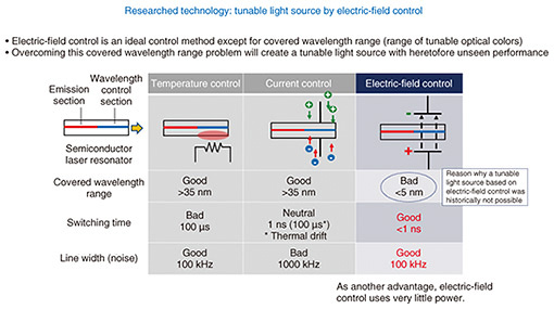
Rising Researchers Vol. 21, No. 1, pp. 7–11, Jan. 2023. https://doi.org/10.53829/ntr202301ri1  “Tunable Light Source by Electric-field Control” Technology for High-quality, Low-latency CommunicationsAbstractThe Innovative Optical and Wireless Network (IOWN) proposed by NTT envisions a future of low-latency, high-quality, and high-speed communications, but making this vision a reality will require a rapid evolution of optical communication devices. In particular, given the increase in network connection devices driven by recent advances in the Internet of Things and the emergence of communication applications with high real-time characteristics, the power consumption and latency of the communications infrastructure have become major issues throughout the world. We talked with NTT Distinguished Researcher Yuta Ueda about “tunable light source by electric-field control” technology as a solution to these issues. Keywords: tunable light source, electric-field control, optical sensing Creating a totally new optical system through wavelength control by an electric field—Dr. Ueda, what type of technology is “tunable light source by electric-field control”? Simply speaking, “tunable light source by electric-field control” is a technology for controlling the color of light by voltage for use in optical communications. The wavelength of light corresponds to color when talking about visible light, and various types of colors can be used in optical communications. For example, if we assign signal A to the color red and signal B to the color green, different signals can be carried on lasers of different colors and input into a single optical fiber. In this way, communication capacity can be increased by many times on the basis of color, which is one advantage of optical communications. In the past, the requirement placed on wavelength-tunable light sources was that preferred colors be output from only one type of semiconductor chip. In this way, the laser chips prepared by telecom operators could be commoditized, thereby reducing inventory and lowering the cost of communication operations. Furthermore, in addition to meeting this inventory-reducing objective, an increase in network connection devices due to the expansion of Internet of Things systems has been making the power consumed for controlling optical wavelengths a problem as well. Here, while the means of decreasing power has fundamentally not been on the physical level, it has nevertheless been an issue of concern in this field. In recent years, moreover, attempts have been made to not only increase the types of optical wavelengths in a tunable light source but also to express new functions by dynamically switching wavelengths in the middle of optical communications. For example, if sunlight, which includes a variety of wavelengths (colors), is passed through a prism, the path that light takes will differ for each color. From this fact, the switching of optical communication paths by dynamically changing wavelengths can be imagined. Simply passing light through a prism completely negates the need for complicated electrical control. In other words, making wavelengths correspond to optical paths will enable high-speed, low-power path control. This phenomenon of driving wavelengths at high speed is not limited to communications—it can also be applied to sensing. For example, the keyword LiDAR (light detection and ranging) has been appearing frequently in newspapers and other media of late as a new optical system having many possibilities. However, semiconductor lasers suffer from high laser noise when driving wavelengths at high speed, and achieving both high-speed and low-noise characteristics as demanded of new optical systems has historically been difficult in either communication or non-communication applications. “Tunable light source by electric-field control” is technology that can resolve these issues. The main point of this technology is to control optical wavelengths by using voltage instead of current when applying an electrical signal. There are various advantages to controlling optical wavelengths by voltage, one being very small power consumption. As learned in middle-school science courses, electrical power is the product of voltage and current, but voltage-based control, to put it another way, means that current is unnecessary (zero). So, simply speaking, it means that the power used for controlling wavelengths can be made very close to zero. In addition, voltage has the property of acting very fast upon a semiconductor so that voltage-based control can be expected to enable high-speed wavelength control. Moreover, it also means no generation of current—frequently the source of noise in semiconductor devices—so that deterioration due to laser noise accompanying wavelength control is small. As a result, voltage-based control can be said to be superior to existing technology in terms of power consumption, high-speed control, and noise, so research has been focusing on whether it can truly solve the various issues that have so far affected optical systems. A tunable light source by electric-field control has many advantages as described above, but it has been considered to be impossible in practice. The reason for this is that a tunable light source based on voltage control has an extremely narrow range in which wavelengths can be changed, which means that a practical wavelength-tunable function cannot be achieved. In response to this problem, we combined optical semiconductor technology researched by NTT over many years with an original semiconductor optical filter circuit that I invented, enabling us to get as far as a proof-of-principle test for a low-power, high-speed, and low-noise tunable light source using the advantages of electric-field control while achieving a practical wavelength-tunable range. —Specifically, what kind of method do you use to operate a tunable light source by electric-field control? At NTT laboratories, I originally belonged to a team in the technical field of modulated light sources, and I feel that I am still applying the experiences and ideas from that time to my present research. A modulated light source is a semiconductor chip that integrates a laser light source with a modulator that places a signal on the laser output from that light source. In this team, we took up wavelength multiplexer technology for combining the light from multiple modulated light sources of different laser wavelengths. As I mentioned earlier, inputting optical signals of multiple wavelengths into a single optical fiber can increase communication capacity. However, from a different perspective, a wavelength multiplexer can also be used to extract a single wavelength from multiple wavelengths. That is to say, a wavelength multiplexer also has the property of being used as a wavelength filter. There are many types of wavelength multiplexers, but in the type of wavelength multiplexer that we were researching at that time, we noticed that wavelength-selection rules were highly sensitive to electrical signals and that a practical wavelength filter could be achieved even for signals not suitable for wavelength control such as voltage signals. “Tunable light source by electric-field control” technology that applies this characteristic generates light of different wavelengths by applying voltage to the original semiconductor filter circuit that I invented and changing that wavelength-selection rule. Of course, technology that changes the wavelength-selection rule by applying an electrical signal to a filter already exists. For example, there are techniques that warm the semiconductor or make current flow. These techniques, however, consume much power in wavelength selection and suffer from the problem that achieving both high-speed wavelength changing and low-noise laser operation is difficult in principle. Electric-field control can solve the above problems all at once, but as I described earlier, there was the problem of obtaining a practical wavelength-tunable range, so achieving a practical device was not yet attainable. With this being the case, we took up the challenge of achieving a tunable light source having a practical wavelength-tunable range even when using electric-field control by applying the ideas that arose in the modulated light source project. As a result, our prototyped tunable light source is able to keep laser noise (line width) sufficiently low in actual use compared with conventional control-by-temperature technology while increasing the speed of wavelength control by as much as one million times. This prototype also exhibits a practical wavelength-tunable range, which suggests this technology can greatly contribute to high-performance optical communications and optical sensing in the future. Moreover, the power used for changing wavelengths is less than 1/10 the conventional value, which means that further power savings can be expected when considering the reduced burden on external circuits. This can solve the present energy problem in communications and contribute to a significant decrease in communication costs (Fig. 1).
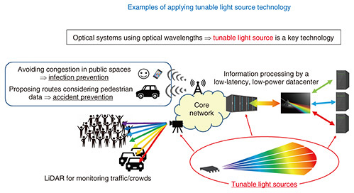
Solving many social problems and creating the IOWN future—Please tell us your outlook for the future using tunable light sources by electric-field control. One objective of the All-Photonics Network (APN) within the Innovative Optical and Wireless Network (IOWN) vision proposed by NTT is to increase power efficiency by 100 times to achieve low power consumption. There is consequently the prospect of using tunable light sources by electric-field control as the platform technology of APN from the viewpoint of achieving a low-power optical network. The idea here is that controlling wavelength tuning by an electric field can reduce the power and costs involved in optical communications and help expand the potential of an information-processing platform in no small way. Additionally, from the viewpoint of low noise and short switching time, achieving other APN objectives, namely, low latency, large capacity, and high quality, is also an outlook for the future. Application to non-communication fields such as optical sensing can also be envisioned. For example, Digital Twin Computing within the IOWN vision converts the real world into a computer society for the sake of data processing with the aim of disseminating beneficial information for society. This process could contribute, for example, to infection prevention and accident prevention in public spaces. Here, “converting the real world into a computer society” is surely the domain of sensing technology. We can therefore expect “tunable light source by electric-field control” technology to serve as an “eye” of the digital world on the real world. In this way, we are aiming for technology that can solve a wide variety of social problems in both communication and non-communication fields and help enhance the lives of many people (Fig. 2).
—Dr. Ueda, can you leave us with a message for researchers and students? At NTT, you can do your work based on the concept of “Wouldn’t the world change if we had this technology?” On top of that, I feel that doing research at NTT can be quite interesting. This is because it’s a place where we ourselves can add finishing touches to our research results up to the practical level and even engage in the device business by selling devices, receiving feedback, and continuing with device development. In short, NTT enables researchers to be widely involved in research, development, and business. I should mention here that all of these schemes are not necessarily carried out within NTT laboratories—the ability to collaborate with outside partners as needed is a key strength of NTT. Of course, writing papers and spreading the word on NTT’s technical capabilities is important work, but in the field of optical semiconductors that I am involved in within NTT laboratories, it is particularly important to perform research repeatedly and make results practical to create new social value all under the idea of “for the world and for people.” I feel that if someone has a need for a certain type of technology and is willing to pay for it, then I have a very worthwhile role to play in this world. From here on, in addition to my research on “tunable light source by electric-field control” technology that I introduced here, I would like to make good use of a wide array of technologies and ideas in all sorts of scenarios and contribute to the creation of a society filled with people leading happy lives. At present, I am conducting device research in the field of optical semiconductors, but in this field, many researchers come together each with a set of specialized skills to conduct research on a daily basis with the aim of creating a single device. Of course, this research and partners too includes overseas institutions. In this process, I feel strongly that “team power” is vitally important for making research proceed smoothly. There is no way that a single individual can perform device research, so it is essential that research be performed in a cooperative manner while respecting people with specialized skills and learning many things from others. In this regard, diversity has recently become an important theme in society, and I too recognize its importance, but in a research project, and particularly in a project that assumes development of a practical product, there are many times in which a single decision is finally made out of necessity, which can easily generate some conflict. In such a situation, it is very difficult to achieve both “decision-making as a project” and “diversity for deepening research discussions,” but I feel that an approach that attempts mutual understanding while seeking compromise among people with different ways of thinking is very important. Of course, a major premise here is that it is exactly a group of individual researchers having their own opinions and interests that constitutes team power. I don’t think that a researcher who does not have ideas on one’s own field of specialty can actually be called a researcher. When I was a student in a master’s program, I was told by an academic advisor, “When you investigate something thoroughly when young, you come to have a different view of things from then on.” Then, with this advice in hand, I went on to a doctor’s program. I would like young researchers who are reading this to place importance on one’s own gut feelings and to pursue one’s research in an all-out, devoted manner. I think that it is more fitting to think of research as one’s consuming interest than simply work. If you truly like something, you can continue to do it with all-out passion and devotion. For this reason, I would like researchers, while still young and highly sensitive, to place importance on what they feel gives them great pleasure. Today, there is much activity in semiconductor research around the world, but in Japan, where fierce competition makes conditions severe and less than optimistic, it is NTT laboratories that provide a blessed environment for research. To young researchers who will take on the burden of future challenges, I say, “Let’s work together as colleagues in creating the future of communications.” ■Interviewee profileYuta Ueda received his Ph.D. in electrical engineering from the Graduate School of Waseda University in 2011. He served as a research fellow of the Japan Society for the Promotion of Science during his doctoral course. He joined NTT in 2011 becoming a member of NTT Photonics Laboratories. He has been an NTT Distinguished Researcher at NTT Device Innovation Center and NTT Device Technology Laboratories since 2022 engaged in the research of semiconductor tunable light sources. He received the Institute of Electronics, Information and Communication Engineers (IEICE) Young Researcher’s Award in 2012 and the IEICE Best Paper Award in 2022. He has been a visiting associate professor at Kyushu University since 2020. |


