|
|||||||||
|
|
|||||||||
|
Feature Articles: Plasmon Control Technology Vol. 21, No. 5, pp. 21–24, May 2023. https://doi.org/10.53829/ntr202305fa2 Electrical Control of Plasmon Reflectivity in GrapheneAbstractProperties of plasmons in graphene can be controlled electrically. My research colleagues and I have used this feature to verify that plasmons of desired frequencies can be excited in electrically specified regions. This technology can be applied to plasmonic devices such as waveguides and switches. Keywords: plasmon, graphene, electrical control  1. Graphene plasmonsPlasmons are collective oscillations of electric charges that have shorter wavelengths than electromagnetic waves at the same frequency and can be confined to regions below the diffraction limit. The technology for manipulating plasmons in nanoscale regions is referred to as plasmonics. Plasmonics has been used in practical devices such as biosensors, as described in the article, “Overview and Prospects for Research on Plasmons in Two-dimensional Semiconductor Systems” in this issue [1]. While surface plasmons excited on metal surfaces are commonly used for plasmonics experiments, they have limitations due to significant losses and poor controllability. These drawbacks have hindered the practical implementation of nanophotonics in which plasmons are used to transmit information in nanoscale structures. Graphene is attracting attention as a plasmonics material that can overcome these problems. Graphene plasmons are known to have low loss in the terahertz and mid-infrared frequency range. Another advantage is that they have a shorter wavelength than metal surface plasmons, which enables them to be confined in smaller regions. Specifically, electromagnetic waves converted into graphene plasmons can be confined to regions 1/1000th the wavelength of the electromagnetic waves. Moreover, the relationship between the wavelength and frequency of graphene plasmons varies with the charge carrier density, providing functions that are not available with metals, such as electrical control of the propagation speed and wavelength of the plasmons by gating. These advantages are expected to pave the way for electrically controllable nanophotonics and new applications, such as electrically tunable metamaterials*1.
2. Electrical control of graphene plasmonsThe relationship between the graphene plasmon wavelength (λ) and frequency (ƒ) varies with the charge carrier density (n): λ ∝
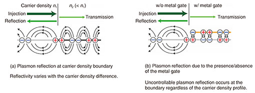
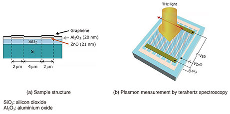
3. Demonstration of graphene plasmon controlThe results presented in this article indicate that the confinement and reflection of graphene plasmons can be controlled electrically by using a high-resistivity zinc oxide (ZnO) thin film instead of metal as the gate material, thus avoiding the uncontrollable reflection caused by the metal gate [2]. The screening effect that is inherent in metal gates can be suppressed when the resistance of the gate electrode is high enough that the charges in the electrode cannot follow the oscillatory electric field at plasmon frequencies. To attain this condition, my colleagues and I used 20-nm-thick ZnO with high resistivity that was attained by adjusting the growth temperature as the gate material. The sample used in the experiments had a two-layer gate consisting of a ZnO thin film processed into strips of 2-µm width and 4-µm spacing on a low-doped silicon (Si) substrate (Fig. 2(a)), enabling independent control of the carrier density of graphene on the ZnO gate and Si gate (nZnO and nSi). The plasmonic response in this sample was examined by irradiating terahertz light with an electric field perpendicular to the strips and measuring the transmission spectrum (Fig. 2(b)).
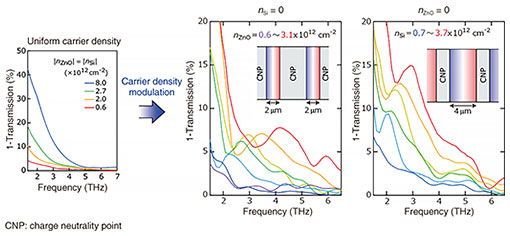
Figure 3 shows the extinction spectra of this sample in the terahertz range. When the carrier density is uniform, the absorption of terahertz light by graphene increases monotonically with decreasing frequency. This is typical behavior observed in pristine graphene, indicating the absence of uncontrolled plasmonic reflections caused by the ZnO gate. However, a peak appears in the spectrum when the ZnO gate and Si gate are adjusted such that the carrier density in either region is set to zero (at the charge neutrality point). Because plasmons are not excited in the region at the charge neutrality point, the spectrum peak can be attributed to plasmon resonance in a cavity formed in a region where the charge density is non-zero. We also succeeded in changing the resonance frequency by using the gate. This shows that it is possible to excite plasmons at the desired location and frequency by adjusting the gate voltages. This active spatial control of plasmon excitation can be applied to waveguides, switches, and resonators.
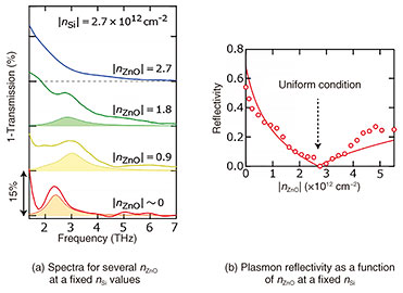
Continuously tuning of the plasmon reflectance at the boundary is also possible by varying the difference between nZnO and nSi. Figure 4 shows spectra for several nZnO values at a constant nSi. As the density difference is increased from a uniform condition, the resonance peak increases with increasing reflectivity. The experimentally obtained plasmon reflectivity (red line in Fig. 4(b)) is consistent with Fresnel’s law
4. Future prospectsThese achievements provide a platform for implementing the theoretical concept for electrically controllable plasmon circuit. For future work, we plan to advance to experiments on directed plasmon propagation with controlled velocity and phase. References
|
|||||||||