|
|||||||||||
|
|
|||||||||||
|
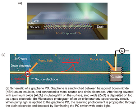
Feature Articles: Plasmon Control Technology Vol. 21, No. 5, pp. 25–29, May 2023. https://doi.org/10.53829/ntr202305fa3 Ultrafast Optical-to-electrical Conversion Processes in GrapheneAbstractGraphene photodetectors have gained significant interest due to their predicted high sensitivity and rapid electrical response to broadband light, offering the potential for superior performance compared with conventional semiconductor devices. However, the experimental evaluation of the operation speed under a zero-bias voltage has been hindered by challenges associated with device architecture and measurement instrumentation, restricting the characterization of graphene’s intrinsic dynamics and clarification of its operating mechanism. This article presents an ultrafast graphene photodetector developed at NTT laboratories, detailing the measurement technology and operating mechanism. Keywords: graphene, photodetector, terahertz electronics  1. Graphene as an optical-to-electrical conversion devicePhotodetectors (PDs) play a crucial role in optical information communications and sensors by converting optical signals into electrical signals. Developing a PD that operates at high speeds for broadband optical signals creates new opportunities for advanced information processing through optical sensors and receivers working across a wide range of frequencies. This requirement can be satisfied with graphene, a promising material that exhibits high efficiency with its ability to absorb 2.3% of incident light with a single atomic layer and operate in an ultrawide frequency band, from terahertz to ultraviolet light [1]. The photothermoelectric (PTE) effect enables graphene PDs to operate at zero bias, which is essential for low power consumption and improved signal-to-noise ratio. However, previous research on graphene PDs has limited the experimental operating speed under zero bias to around 70 GHz [2], far from the theoretical expectation of 200 GHz. The limitations in device structure and measurement systems have hindered the investigation of the intrinsic response of graphene and the clarification of its operating mechanism, leading to a lack of design guidelines for maximizing the performance of graphene PDs. Therefore, the demonstration of 200-GHz operation speed and the elucidation of the physical properties of graphene, including the optical-to-electrical (OE) conversion mechanism, is crucial for further developments in graphene PDs. 2. Ultrafast photocurrent detection based on a novel device architecture and measurement approachUltrafast OE conversion in a graphene PD requires a device design that facilitates prompt tracking of incident light signals and a measurement technique capable of high-speed photocurrent detection. To meet these requirements, we used a zinc oxide thin film as a gate material to eliminate the current delay caused by capacitive coupling (Fig. 1(a)) and used on-chip terahertz spectroscopy [3] for photocurrent readout (Fig. 1(b)). The OE conversion efficiency of graphene PDs using the PTE effect varies significantly with the charge density. Thus, a gate structure must be integrated into the device. Because the gate electrode must possess high conductivity, gold is commonly used as the gate material; however, this limits the operating speed to below 100 GHz due to unwanted capacitive coupling. We addressed this issue by using a zinc oxide thin film, which enables control of the high-frequency response by controlling growth conditions. This material possesses a unique combination of being a good conductor for direct-current signals while being transparent at terahertz frequencies [4]. As a result, we successfully eliminated the capacitive coupling-induced current delay. The high-speed oscilloscopes commonly used to read out the photocurrent struggle to measure response faster than 100 GHz because of the bandwidth limitation of the electronics. However, we overcame this challenge by using on-chip terahertz spectroscopy, which enabled us to measure the ultrafast response of the graphene PD with a measurement bandwidth approaching 1 THz through the detection of photocurrent using an on-chip photoconductive (PC) switch. The photocurrent generated by irradiating the graphene PD with a pump pulse (femtosecond laser pulse) propagates through the drain electrode to the PC switch (Fig. 1(b)). Because the PC switch becomes conductive when irradiated by the probe pulse (also femtosecond laser pulse), the signal flows to the ammeter only when the generated photocurrent and probe pulse overlap in time. Therefore, measuring the photocurrent waveform with extremely high time resolution is possible by constantly changing the time difference between the pump and probe pulse. Our innovative device architecture and measurement approach have enabled us to explore the ultrafast OE conversion mechanisms in graphene, which was previously unachievable using conventional methods.
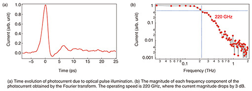
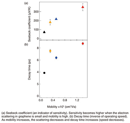
3. Overview of the OE conversion processes in grapheneThe photocurrent waveform of the fastest response among measured signals is shown in Fig. 2(a). The various frequency components of the photocurrent obtained by the Fourier transform (Fig. 2(b)) show that the 3-dB bandwidth of the graphene PD reaches 220 GHz, more than three times the 70 GHz reported previously and exceeding the theoretical expectation of 200 GHz. This is the first successful extraction of the intrinsic response of graphene unimpeded by device structure or measurement method. To investigate the physical process that determines the dynamical response of the photocurrent, we first focused on the decay time of the photocurrent by fabricating multiple devices with different graphene mobilities. Figure 3 shows that lower graphene mobility is associated with shorter decay times. This result suggests that the decay of the photocurrent in graphene is caused by a decrease in the electron temperature in graphene, which is increased by light irradiation. Because of collisions between acoustic phonons and defects, a sample with lower mobility and more defects loses more energy in a single collision event, resulting in faster decay times. However, the Seebeck coefficient, which corresponds to PD sensitivity, increases as mobility increases (Fig. 3), so there is a tradeoff between bandwidth and sensitivity in graphene PDs. Therefore, it is necessary to select optimal graphene mobility in accordance with the intended application.
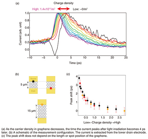
To identify the mechanism that determines the photocurrent generation and propagation response (Fig. 4(a)), we investigated the dependence of the photocurrent on the charge density. The results indicate that a decrease in charge density produced a delay in the peak position of about 4 ps. Such a significant peak shift is unprecedented and provides important clues for understanding the OE conversion processes. We can consider two possible causes: 1) the propagation time of the photocurrent through graphene changes or 2) the time for photocurrent generation after light irradiation changes. To test the first possibility, we measured the peak shift for various device lengths and the irradiation position of the pump light (Fig. 4(b)). All the results fall on a single curve (Fig. 4(c)), indicating that the photocurrent propagation time in graphene is too short to be measured, so the cause of the peak shift must come from the change in the photocurrent-generation time. The ultrashort propagation time in a graphene PD results from its gapless nature. The absence of a bandgap in graphene allows the electric field created by light irradiation to propagate at the speed of light, instantly displacing the electrons near the electrode and generating an immediate flow of current without the need for propagation. The time variation in photocurrent generation is due to the PTE effect, which transforms the electron temperature into a voltage. This means that the non-equilibrium electron state created by the light irradiation quickly settles into a Fermi-Dirac distribution through intraband electron scattering. Our results also indicate that the time it takes for thermal equilibrium is highly dependent on the charge density of the graphene. These findings provide a comprehensive understanding of the ultrafast OE conversion processes in graphene, including the generation, propagation, and decay of photocurrent upon light irradiation [5].
4. Future developmentThe results presented in this article indicate the high potential of graphene as a material for broadband, high-speed PDs. However, our fabrication process of manually exfoliating graphene from graphite is not suitable for mass production. While the quality of graphene deposited over a large area has been historically inferior to that obtained through exfoliation, the gap is closing as deposition techniques continue to improve. Future studies will focus on evaluating PDs that use large-area graphene to facilitate mass production. Additionally, research in the field of creating novel materials by stacking graphene and other two-dimensional materials could be applied to further enhance the operating speed of PDs. The results of this study could be used to generate, control the propagation of, and detect graphene plasmons in the terahertz range. This opens up the possibility for on-chip handling of plasmon signals, bringing us closer to the goal of creating plasmonic circuits. References
|
|||||||||||