|
|
|
|
|
|
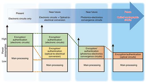
Rising Researchers Vol. 22, No. 5, pp. 12–17, May 2024. https://doi.org/10.53829/ntr202405ri1  Optical Cryptographic Circuit Technology Consisting of Optical Logic Gates for a Secure Information-processing PlatformAbstractThe next-generation communication network driven by optical technology will be achieved in the sixth-generation mobile communication system (6G) of the Innovative Optical and Wireless Network (IOWN) era promoted by NTT. However, a problem of concern here is cryptographic technology. For example, even if optical circuits can be achieved, cryptographic operations in their present form would generate delays or excessive power consumption preventing the advantages of optical technology from being fully used. To solve this problem, NTT is researching technology for replacing the complex processing of cryptographic operations traditionally performed by electronic circuits with optical cryptographic operations. In this article, we talk with NTT Distinguished Researcher Junko Takahashi who devised an “optical-operations technique” supporting the IOWN era and implemented “optical cryptographic circuits.” We hear about the present state of research in optical cryptographic technology and the future outlook for this research. Keywords: optical cryptographic circuit, All-Photonics Network, photonic disaggregated computing platform  Achieving a secure APN through innovative cryptographic technology—Dr. Takahashi, can you first explain “optical cryptographic circuit technology consisting of optical logic gates” for us? “Optical cryptographic circuit technology consisting of optical logic gates” that I am researching is technology that achieves cryptographic operations traditionally performed electronically by optical circuits. The catalyst for beginning this research was NTT’s major promotion of its Innovative Optical and Wireless Network (IOWN) vision in the years 2019–2020. At that time, I thought “Couldn’t innovative security technologies including cryptographic technology be created by applying optical technology, the key to IOWN, in the research of cryptography and security technology that I had so far been involved in?” This was the origin of my research theme. In the past, it was common sense to execute complex processing like cryptographic operations electronically. In IOWN, however, the aim is to achieve low latency and low power consumption by replacing the computing environment including servers and all sorts of electronic devices with devices based on optical technology and interconnecting them by an optical network. Achieving the processing of operations by optical technology, however, is not without its problems. Specifically, if only cryptographic operations were to be implemented on electronic circuits, the result would be high overhead (load) due to optical-to-electrical conversion causing a drop in operation performance throughout the computing environment. My new research therefore began with “optical cryptographic circuit technology consisting of optical logic gates.” Thinking that operations with even lower latency and lower power consumption could be achieved and the load on the environment decreased by implementing even cryptographic operations using light in the All-Photonics Network (APN) of the IOWN vision, I began to fabricate and research cryptographic circuits using optical circuits (Fig. 1).
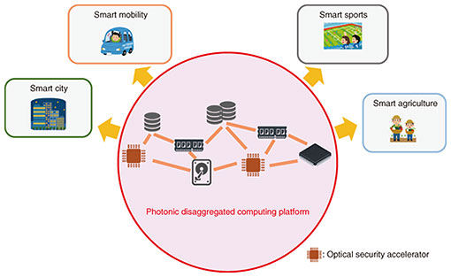
—What kinds of difficulties have you encountered in actual research? On starting out with my research, I thought that I could implement optical cryptographic circuits simply by combining existing optical-operations devices. I assumed that this could be easily achieved in about the same period as the design and fabrication of electronic circuits. In actuality, however, I found in the course of my research that there were a variety of physical problems different from theory. To begin with, optical-operations devices necessary for cryptographic operations were still in the development stage throughout the world, and even the devices that were ready for use had limitations in how they could be used. Achieving fundamental cryptographic techniques on optical circuits requires that cryptographic processing be configured with multiple logical operations. However, optical-operations devices that can presently be used have limitations such as the inability of performing multiple logical operations. In addition, there are devices that are still in the development stage in terms of performance requirements such as latency and power consumption. So the present state of affairs is that current devices cannot at all meet the numerical targets set for APN. Therefore, one challenging point in my research was how to configure existing complex cryptographic functions using optical-operations devices that are limited in their operation. Additionally, peripheral circuits such as memory and registers required for executing cryptographic operations have not yet been developed with optical technology, so it was necessary for me to implement them on electronic circuits. Therefore, another challenging point in terms of achieving low latency and low power consumption was how to demonstrate maximum performance by combining optical circuits and peripheral circuits in some way. Furthermore, in terms of fabricating optical devices, all processing including the drafting of designs and fabrication of circuit chips and peripheral circuits would take a very long time in units of years, so that also was a major obstacle that I had not expected until I began this research. For this reason, I had to search out devices that could be manufactured in a relatively short period of time and from which I could extract good performance. Circuit chips, moreover, could not be modified once fabricated, so there was no going back in this regard, and as a result, I had to carefully consider how best to configure the circuits and what method to use in manufacturing them. Finally, using optical-operations devices with good performance had a tendency to expand the overall circuit scale, so determining how to minimize this also became a major issue. —Please tell us about some of your research achievements to date. In research up to the present, I have devised an operations technique that achieves a nonlinear operation—an important type of function in cryptographic operations—using a technique called “one-hot encoding.” Specifically, I have fabricated an optical cryptographic circuit based on silicon photonics technology targeting a function that performs 4-bit input/output table conversion. Basically speaking, this one-hot encoding technique performs operations based on optical wiring. Unlike electronic circuits, optical wiring has no wiring resistance making low-latency operations possible. In addition, while ordinary cryptographic operations use bit representations (‘0’ or ‘1’), such bit representations must be converted to hexadecimal (base 16) representations to use the one-hot encoding technique. Additionally, by using Mach-Zehnder optical modulators here, which among optical-operations devices are relatively easy to implement, and by combining these optical modulators with optical wiring, I have implemented an optical circuit chip having a cryptographic nonlinear function as a world’s first. To test the operations performed by this optical circuit chip, I also fabricated an optical device that combines the optical circuit chip with an electrical section and confirmed that the nonlinear function could indeed operate correctly. This optical device features the ability of performing an operation with extremely low latency on the order or several tens of picoseconds after the electrical signals controlling the optical modulators (input signals to the nonlinear function) are input, which I believe will make a big contribution to meeting APN targets. “Light” shines exactly on places that appear to be unrelated to research—Please tell us your outlook for this research going forward. In circuits that have so far been researched and developed, input is made up of electrical signals while output consists of an optical signal, which means a photonics-electronics convergence circuit. Today, however, with the aim of achieving low-latency and low-power operations, I am in the process of fabricating a new type of optical circuit chip achieving a nonlinear function having optical signals as both input and output using optical-operations devices called Y-gates and Ψ-gates that enable logical operations. I confirmed through experiment that this optical circuit as well could perform operations correctly, so I feel that we are making steady progress toward APN of the future. As for future developments, considering that a “photonic disaggregated computing platform” featuring distributed hardware resources is scheduled to be established in the 2030s, my aim is to achieve a computing environment that implements optical cryptographic operations circuits so that anyone can safely use this new communications platform (Fig. 2). In terms of numerical targets, I am working daily in my research to fabricate circuits that can operate at “1/1000 the latency” and “100 times more energy efficiency” of conventional electrical cryptographic operations circuits. Further into the future, moreover, I would like to fabricate optical cryptographic circuits that can be used not only in a terrestrial computing environment but also in a computing environment in space (Space Integrated Computing Network) and to develop them into a technology that will make a major contribution to new next-generation communications platforms.
The research that I pursued was unprecedented, and reactions from the outside when I started out were all skeptical in the manner of “This is like magic—is it even possible?” For sure, in 2019 when I began this research, people who thought that only the network portion of the communications platform consisted of optical communications were in the majority, and devices that could implement some operations with light were still in the development stage. Under these conditions, it was natural to have doubts about replacing cryptographic circuits originally designed with digital circuits with light. However, when demonstrating for the first time that cryptographic operations could be performed with light and announcing that achievement, I received favorable responses from many people, and I remember how happy I was that “I was able to change even if only a little the common belief that such a thing was impossible.” At present, it is still not possible to operate all cryptographic circuits by light, but I would like to take on research that even more people agree with by gradually demonstrating the possibilities of optical circuits. —What is your impression of NTT laboratories? NTT Social Informatics Laboratories that I belong to deals not only with basic cryptographic technology but also with a wide range of research themes related to social systems. These include security-related research of cyber-attack countermeasures technology targeting attacks made against the network and Internet-of-Things systems and of data protection technologies such as secure computation technology and artificial intelligence security, research aiming for the well-being of everyone, and research related to legal systems and ethics. I myself was engaged in the research of cyber-attack countermeasures technology separate from the research of cryptographic technology for about six years before beginning my present research. In this way, I can get involved in a variety of research themes related to social systems at NTT Social Informatics Laboratories. I can even get involved in cyber-security research after completing my work in cryptographic-related research themes and then return once again to cryptography. In short, NTT Social Informatics Laboratories creates an unconstrained, relaxed atmosphere in which a researcher can move in and out of different research themes. For researchers having interests in many fields, I feel that the Laboratories provides a very attractive environment. I also feel that a strong point of NTT Social Informatics Laboratories that deals with a variety of research themes is the ability to easily consult with nearby researchers whenever encountering a problem outside of one’s specialty during research. I once encountered a problem related to legal matters and ethics in my research and I was faced with a situation in which I had to interpret this problem. Since this was naturally outside of my specialty, I was very distressed, but since a researcher who dealt with research themes related to the law and ethics was nearby at the laboratory that I belonged to at that time, I was able to consult with that person immediately on how to solve my problem and to continue with my research smoothly. In this way, providing a means of quickly solving problems outside of one’s range of research when a problem arises is truly an NTT strong point. I am very grateful for this environment that allows me to get on with my research with a sense of speed. —Dr. Takahashi, please leave us with a message for researchers, students, and business partners. Generally speaking, we can think of the work of research as mainly consisting of writing papers, making presentations at academic societies, and submitting patent applications, as well as the development of research results into business applications. However, ever since I entered the company, I’ve also placed importance on everything I can do on my own, that is, processes outside of research that naturally arise in the course of conducting research. For example, while working on cyber-attack countermeasures technology for cars several years ago, we had to evaluate the characteristic functions of cars from the viewpoint of security, and that required that we get our hands on an automobile manufactured in a specific period having certain functions related to driving. Since such an automobile was of a model no longer sold as a new car, we had to contact used-car dealers all over Japan and eventually found one that had what we needed, so we went out there and conducted negotiations and procedures ourselves. And after that, we of course had to maintain the car ourselves on a daily basis. We also selected various types of equipment that we needed to carry out this research, made a field trip to the only place in Japan where such equipment was currently installed to gather information, and did everything ourselves that was needed for installing the equipment at NTT including negotiations with installers and in-house procedures related to installation work. Such a process, to be sure, does not appear at first glance to be directly related to the work of research. However, I think that taking on everything by the sweat of one’s brow can reveal the backside of an industry and bring the overall picture into view. In particular, when jumping into a research field of an industry different from one’s own research field, one must learn the implicit features of that industry such as what is taken to be “common sense” and what “manners” are practiced. Armed with this knowledge, it often becomes easier to interact with people in another field. For this reason, I always “do everything myself to the degree possible” in my research work. Research of optical cryptographic circuits using optical logic gates that I am now working on requires many processes. In addition to theoretical studies of cryptography, it involves the fabrication of optical circuit chips and optical devices based on electrical circuits, the fabrication of peripheral devices, and construction of environments for performing proof-of-principle experiments on circuit chips. Since I cannot do all of this on my own, I greatly appreciate the involvement of many people who help me to move my research forward. It is very reassuring for me that NTT laboratories, which bring together many specialists in fields ranging from theory to devices, will continue to provide an environment in which I can give shape to my own ideas and thoughts. In such an environment, I would like to work with as many researchers, students, and business partners as possible in providing base technologies for configuring a secure information infrastructure of the IOWN era. To any readers who are interested in this endeavor, I would say, “Let’s work together in taking on the challenges of the future.”
■Interviewee profileJunko Takahashi received her B.S. in physics in 2004 and M.S. in physics and applied physics in 2006 from Waseda University. She entered NTT in 2006 and received her Ph.D. in engineering from the Graduate School of Informatics and Engineering, University of Electro-Communications in 2012. Her specialty is hardware security. She has previously been engaged in side-channel-attack countermeasures technology, automobile security technology, and embedded security technology. She is presently engaged in the research of optical cryptographic circuits at NTT Social Informatics Laboratories. She is an Invited Researcher at the Cyber Physical Security Research Center, National Institute of Advanced Industrial Science and Technology (AIST). She is a member of the Institute of Electronics, Information and Communication Engineers (IEICE) and Information Processing Society of Japan (IPSJ). She has been an NTT Distinguished Researcher since 2023. |