An optical version of Moore’s law: membrane optical devices
—Would you tell us about the research you are currently conducting?
Since joining NTT in 1988, I have been researching photonics-electronics convergence devices, focusing on technologies for the integration of heterogeneous materials. NTT announced the concept of the Innovative Optical and Wireless Network (IOWN) in 2019, and photonics-electronics convergence devices are key for implementing the All-Photonics Network (APN), a component of IOWN. Such devices will contribute significantly to reducing power consumption. Regarding photonics-electronics convergence in IOWN, we have thus far developed devices for replacing electrical-based interconnections between racks and between boards with optical interconnections (first and second generations, respectively). We are currently conducting research and development and practical applications of devices for optical interconnections inside a board (third generation), inside a package (fourth generation), and inside a chip (fifth generation). To put these devices into practical use, the development of an integrated circuit (chip) that can cope with the explosive increase in the number of devices while reducing cost and power consumption will be a challenge. Overcoming this challenge is what we are trying to achieve Moore’s law—an empirical rule that states the number of devices (such as transistors) mounted on a single chip doubles every 18 months—in optical devices, including light-emitting devices such as laser diodes (LDs), which are essential for optical interconnection.
Moore’s law regarding semiconductors has held true for more than 50 years thanks to the use of large-area fabrication and microfabrication technologies such as silicon complementary metal-oxide-semiconductor. To achieve Moore’s law in optical devices, it is important to use silicon (Si)-photonics technology that uses optical waveguides, etc. using Si. However, optical devices, such as lasers and highly efficient optical modulators, cannot be fabricated using Si; therefore, we fabricate them using indium phosphide (InP)-based compound semiconductors, and large-scale integration of such optical devices is achieved through heterogeneous integration. Integrating Si and compound semiconductors, however, is difficult because they have different lattice constants, which represent the size of the unit lattice of a crystal lattice, and coefficients of thermal expansion, which represent the relationship between changes in length and volume due to changes in temperature. With that difficulty in mind, using Si-photonics technology combining NTT’s proprietary thin-film technology and direct-bonding technology, we developed a thin-film (membrane) directly modulated LD fabricated on a Si substrate as a light source for intra-board optical interconnection [1]. We discussed this LD in the previous interview (September 2021 issue) in this journal.
—How is your research on membrane optical devices progressing?
Regarding membrane directly modulated LDs, our research and development is continuing to increase the number of channels and improve stability and reliability to put them into practical use. We are also researching and developing membrane optical modulators, which do not directly modulate the laser but use the laser as a bias light source and use a separate modulator from the light source with higher speeds and a higher temperature range.
Optical modulators can be classified into two types: phase modulators, which primarily modulate the refractive index, and intensity modulators, which modulate the absorption coefficient. A phase modulator is used as a Mach-Zehnder (MZ) modulator in combination with an MZ interferometer, which measures the phase difference between two parallel beams derived from a single light source. By combining multiple MZ modulators and modulating the phase, intensity, and polarization, it is possible to achieve long-distance transmission with increased capacity exceeding 1 Tbit/s per wavelength. Typical materials used for phase modulators are lithium niobate (LiNbO3), Si, and InP-based compound semiconductors. Due to the increases in traffic, optical interconnections will increase in importance in short-distance transmission (2 km or less) such as in a datacenter. Therefore, it is necessary to reduce the transmitter cost by reducing the device size and integrating many devices on a single chip. Indium-phosphide-based compound semiconductors, which are one order of magnitude more efficient than LiNbO3 and Si, are considered key materials to satisfy this requirement.
Regarding intensity modulators, InP-based compound semiconductors and germanium silicon (GeSi) are typically used. Since intensity modulators use only the intensity change as a signal, the transmission capacity is generally smaller than that of MZ modulators; however, their simple and compact configuration is of importance when a large number of transmitters are required for short-distance transmission. Considering the use of intensity modulators in the 1.3-μm wavelength used in datacenters, there is currently a problem in the crystal growth of GeSi; thus, InP-based compound semiconductors have an advantage.
Figure 1(a) shows a schematic of a photonic integrated circuit we fabricated, which integrates an MZ modulator consisting of a Si MZ interferometer and InP phase modulators with membrane lasers through heterogeneous integration.
By integrating spot size converters (SSCs), which convert the light spot size of a Si waveguide to that of a silicon oxide (SiOx) waveguide, it is possible to efficiently assemble a device with optical fiber by butt-coupling without using a lens. The cross-sectional views of a membrane laser and phase modulator are respectively shown in Figs. 1(b) and (c). Since the lasers for biasing the modulators require continuous light with high output power and stable single-mode lasing, it is important to minimize the optical confinement factor in the laser’s core layer. Therefore, a Si waveguide is placed under the laser’s core layer.
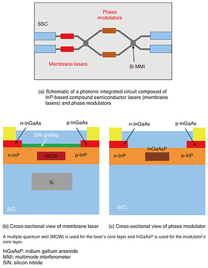
Fig. 1. Photonic integrated circuit composed of InP-based compound semiconductor lasers and phase modulators integrated on Si waveguide.
We also fabricated an electro-absorption modulator (EAM) using InP-based semiconductors. An EAM exploits the phenomenon that the band gap shifts to the longer-wavelength side and the absorption coefficient changes when an electric field is applied to a semiconductor with a band gap near the operation wavelength. Since the EAM directly changes the amount of electric field absorbed, there is no need to use an interferometer such as an MZ modulator, which results in a very simple configuration. These devices (i.e., membrane lasers, phase modulators, and EAMs) will be key for third-generation photonics-electronics convergence and beyond for short-distance, high-throughput optical interconnection.
Due to the above achievements, in 2022, I was elected as an Optica Fellow for “pioneering contributions to ultra-high-speed and low-power-consumption membrane lasers,” and in 2023, I received the IEEE Photonics Society William Streifer Scientific Achievement Award for “contributions to ultra-high-speed, low-power-consumption membrane lasers and their heterogeneous integration.”
Our team is also working on practical application of these devices and accelerating joint research with partners, such as Furukawa Electric, to make these devices have low power consumption and low cost toward developing the third- to fifth-generation photonics-electronics convergence devices for IOWN. We are also conducting joint research on ultrafast directly modulated lasers on silicon carbide (SiC) substrates with Tokyo Institute of Technology, the University of Tokyo, and Keio University, with the aim of achieving the world’s highest performance while developing ultra-low-power-consumption photonic crystal lasers in collaboration with NTT Basic Research Laboratories. We also intend to build an ecosystem for expanding the market for photonics-electronics convergence devices into the fields of computing and inexpensive, high-performance sensing (Fig. 2).
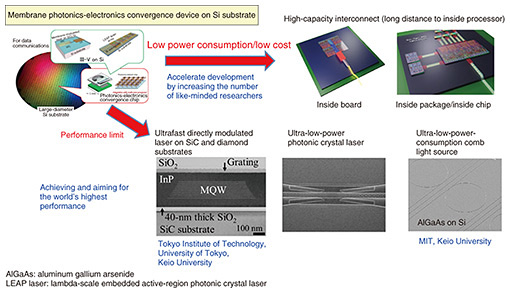
Fig. 2. Development of future technologies.
Everything requires a sense of balance
—What do you keep in mind as a researcher?
In the previous interview, I said that I try to collect information and explain my research to people so that they can understand it, and that mindset has basically not changed. I became an NTT Fellow in April 2023, and that status has made me more aware of my expected contribution to IOWN and the fostering of young and mid-career researchers.
My way of thinking slightly differs between basic research and applied research and practical applications regarding fostering researchers. In regard to basic research, I encourage researchers to have a long-term perspective and proactively take on challenges on the basis of that perspective. When people start to worry about their evaluation within a company, they inevitably pursue short-term results; thus, their perspective becomes short-term. This tendency seems to be especially prevalent among young people. From my experience, basic research takes time—in some cases, 20 or 30 years—to produce results. If we seek short-term results, we will achieve neither significant development nor true results as basic research. That is why we need a long-term perspective. Nonetheless, if we think about it in the long term, we might end up following a set path that is exactly as we originally envisioned. However, due to changes in the surrounding environment, the path is not always pointing in the correct direction, so its trajectory must be corrected, and in some cases, it may be necessary to make major corrections to the trajectory. In that case, by actively taking on challenges, we can expect new discoveries and major progress.
In regard to applied research and practical applications, it is necessary to solve the problems in front of you one by one as a team while taking into account the schedule and your own role within the team, applying teamwork to complement each team member, and polishing your execution ability. My team covers the entire process from basic research to applied research and practical applications, so we need both long-term and short-term perspectives. I therefore strive to encourage each team member to be aware of these two perspectives in accordance with their role.
—You have served on the boards of many international conferences and academic societies. How have those experiences affected researcher development?
At the Institute of Electrical and Electronics Engineers (IEEE), I served as the chair of the Steering Committee of the Si Photonics Conference 2024 and as the board of governors of the Photonic Society from 2023 to 2025. At the Optical Fiber Communications Conference and Exhibition (OFC), I served as the program chair in 2020 and general chair in 2022. For Compound Semiconductor Week 2019, I served as the chair of the Steering Committee. At OFC, while involved in the management of the conference, I noticed that the way of thinking and behavior of people from other countries differs from what Japanese people are aware of. For example, when it comes to supporting women in terms of gender balance, people from Europe and the USA are more proactive and explicit than Japan. They are also careful to maintain a balance among regions such as South America, Africa, and Asia. This was a new experience for me because we in Japan consider the gender ratio, but we are not so aware of regional and other balances.
I often talk to young people about how it is important to know what people around the world—not just Japan—value. To attain such knowledge, it is helpful to get involved in organizing international conferences from a young age, so I encourage them to participate in these activities as much as they can. These activities will help them understand not only technology but also ways of thinking and cultural aspects of people from different countries.
The field of optical devices and photonics-electronics convergence devices is one of the most-advanced fields of research. The number of researchers in this field is still small, thus we have the opportunity to lead the world. We are actively participating in conferences to promote our technology and persuade more researchers to join us in this field. Therefore, the number of people researching something similar to our field will gradually increase, and a new trend will be created. If you are too far ahead and others cannot keep up, you will not be able to make connections with other researchers and will become isolated. However, if you stick too close to others, you are more likely to be overtaken. In other words, it is necessary to strike a balance between these two situations, and I believe that understanding the way of thinking and cultural aspects of people from around the world will help us strike that balance.
—What is your message to younger researchers?
Regarding basic research, I urge young researchers to take a long-term perspective. NTT’s research laboratories are unique in that although they are corporate laboratories, they also conduct basic research. Basic research, which is one of our strengths, is the result of endeavors of ten or more years. Of course, you will make achievements along the way, but they will be mid-term and short-term results as milestones toward achieving the goal in mind from a long-term perspective. These medium- and short-term milestones will satisfy internal evaluations, but focusing too much on them can lead to losing sight of the ultimate goal.
Regarding applied research and practical applications, it is necessary to achieve results while aiming toward short- and mid-term goals. You should therefore change your perspectives in accordance with your current position. Some researchers switch between basic research and applied research and practical applications. For our team, the two are in direct contact. Therefore, it is important to take a balanced approach in understanding each person’s perspective and position.
Reference
| [1] |
T. Hiraki, T. Aihara, T. Fujii, K. Takeda, T. Segawa, and S. Matsuo, “Development of Membrane Optical Modulators for IOWN,” NTT Technical Review, Vol. 20, No. 8, pp. 28–34, Aug. 2022.
https://doi.org/10.53829/ntr202208fa3 |