 |
|||
|
|
|||
|
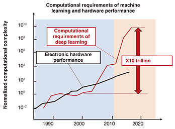
Rising Researchers Vol. 22, No. 8, pp. 13–18, Aug. 2024. https://doi.org/10.53829/ntr202408ri1  Machine Learning Using an On-chip Photonic Neural Network—Changing the Future through Photonic TechnologyAbstractArtificial intelligence (AI) is now entering its fourth wave, and this time, it is penetrating everyone’s daily life and bringing many surprises. However, training an advanced AI model requires a huge amount of resources such as time in units of several months and power equivalent to all of the power consumed by a medium-sized city. To solve this problem, studies are being conducted on AI-model computing using optical circuits that are fundamentally different in principle from past technology. In this article, we talked with NTT Distinguished Researcher Mitsumasa Nakajima about the potential of future photonic technologies and his research on “machine learning using an on-chip photonic neural network” that can greatly reduce the power consumed by machine learning through the use of photonics. Keywords: machine learning, optical circuit, optical computing Revolutionizing next-generation computing technology through the properties of light—Dr. Nakajima, exactly what kind of technology is “machine learning using an on-chip photonic neural network”? In short, “machine learning using an on-chip photonic neural network” is technology that can significantly reduce the amount of power consumed by machine learning through the use of photonics. The background to the research of this technology is the remarkable progress in artificial intelligence (AI) in recent years. The lives of many people in society are already benefiting from AI, but on the other hand, there are still many problems that need to be solved from the viewpoints of calculation speed and power consumption. For example, training an advanced AI model based on an electronic computer currently requires time in units of several months and power on the level of several hundred megawatts (equivalent to the power consumed by a medium-sized city). Since a huge amount of resources are already needed, it has been pointed out that future advances in machine learning will eventually hit a hardware limit by simply extending current technology (Fig. 1).
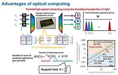
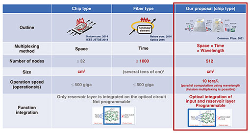
To solve this problem, I am researching AI-model computing using optical circuits as hardware that is fundamentally different in principle from past technology. The reason as to why I began this research in the first place goes back to 2013 during the AI boom of that time. I was hardly aware of all the excitement since I had only overheard people in other departments saying things like “This is really amazing!” Eventually, however, I began to hear similar things from all sorts of people, and I too began to think, “This will no doubt become a major research theme that will somehow bring about a new era.” At that time, I was engaged in the research of optical waveguides and optical communication devices, and I came to focus on “analog matrix operations by light” as a contact point between machine learning and my own research. This was truly a calculation method at the heart of machine learning, so I got the idea that the technology developed for devices like switches incorporated in optical waveguides that I was researching could be used here as well. I then began my research. —What are the advantages of using optical circuits in AI computing? To be specific, making full use of the “space,” “wavelength,” and “time” features of optical operations makes it possible to execute matrix operations at the root of AI models at high speed with low power consumption (Fig. 2). It has been experimentally shown that optical circuits that we have so far fabricated can achieve 1016 calculations per second, which is about 1000 times faster than that of conventional general-purpose central processing units (CPUs), and can decrease power consumption per operation to the picojoule–femtojoule range, which is about one-tenth the conventional level (Fig. 3). Of course, it has been suggested for some time that using light has the possibility of enabling high-speed calculations, but announcing that we have actually demonstrated this to be true at academic conferences and elsewhere has been well received with many people expressing surprise. I have also received invitations like “Let’s try using the optical circuits that you fabricated in communication transmission experiments.” The wide network of fellow researchers that I have been able to cultivate through this research is a driving force behind my research to this day.
—What difficulties have you encountered in your research? The most difficult thing that I had to face occurred when I first started out on this research, since I had no technical experience about machine learning. Fortunately, I was able to start this research with the support of a unique research fund in our laboratory. In this scheme, we can use part of our office hours and budget for our own research topic. Before I took on this research, I was engaged in a single research and development theme along with several tens of other researchers. Once I became familiar with the work that I was placed in charge of, I would proceed with that work as my main line of research. However, since I myself had chosen this research related to machine learning, I had to do everything on my own. I, of course, had to grapple with device-related technology such as device design and evaluation for performing optical computing, but in addition, I had to research machine-learning algorithms. Nowadays, there are plenty of books and know-how related to machine learning, but when I started this research, there was not a sufficient amount of well-organized information. To therefore study up on this field and accumulate knowledge, I began with a trial-and-error process in which I would read journal papers and attempt to reproduce their results. Of course, I couldn’t understand everything by doing only that, so I would sometimes take my questions to neighboring NTT laboratories or to university professors specialized in this field. Looking back, acquiring new knowledge and encountering fellow researchers in this way was a truly valuable experience. —Please tell us about your research vision going forward. In terms of future themes, I would first like to aim for a phase in which members of the computer industry come to use the results of this research. Current optical computing makes use of multiple units of large laboratory equipment, but in the future, I would like to enable optical computing to run at least on the cloud by making further advances in our research and refining the mechanisms involved. Additionally, in terms of optical computing as part of NTT’s Innovative Optical and Wireless Network (IOWN) vision, my aim is to convert communications between electronic computers and between CPUs, memory, etc. to photonics. Once we enter this era, I believe that optoelectronic integrated circuits having a mix of optical circuits and electronic circuits will become commonplace on computers. Then, as the next research stage, my goal will be to achieve practical device technologies that incorporate optical computing functions. Certainly, it’s difficult to perform general-purpose calculations as commonly done on a CPU by optical means, but I think that it will be possible to perform those calculations not conducive to light by electronic means, and conversely, to perform those calculations not conducive to electronics by optical means. Dividing up calculations among electronics and optics in this way will enable general-purpose computational processing to be performed using light. Another goal is to achieve an optical computer that improves power and calculation speed by several orders of magnitude compared with conventional computers. In this regard, I would like to contribute to the ongoing development of computations for ever-expanding AI and to the easing of environmental loads by achieving a dramatic reduction in power consumption. I also plan to search for applications that make good use of the unique features of photonic operations beyond computers. For example, signal processing in optical communications uses many matrix calculations, but it is thought that assisting this processing by optical means can help reduce power consumption and lower delay in communications, so I am studying an expansion of my research into this area. Through these efforts, I hope to contribute to performance improvements in optical computers, to the widespread use of optical computing, and to the creation of optical-computing applications. At present, the number of researchers engaged in the field of computational processing using light is increasing around the world, so I would like to enhance NTT’s presence in this field while continuing to produce research results. Having a mindset that enjoys trial and error and is willing to say “Now I understand what won’t work!”—Please tell us about other research ideas that you would like to pursue. It has only been 80 years since the invention of the transistor, but the electronic computer based on that simple mechanism has come to enrich our lives beyond imagination. Yet, I don’t think that this trend will necessarily continue in the 21st century and beyond. For example, it is thought that bits, neurons, and qbits will become important units of computing in the future. Bits are the units of von Neumann computers, neurons are the units of neural-network operations for AI, and qbits are the units of quantum computers. History has proven that digital electronic circuits are currently the best way to handle bits, but it is not yet known what types of circuits would be best for handling neurons and qbits. Additionally, the conventional idea was to do all bit operations on the same type of circuit (if the operation is electronic, do it all on electronic circuits). However, it is also possible to use different technologies as in using electronic circuits for gate operations and optical circuits for information transfer. In this way, when stepping out of the commonly accepted framework of conventional computers, optical computing becomes an attractive candidate. High-speed and low-power computing for AI using the parallel properties of optical wavelength, space, and time can be provided for neurons while high-speed, room-temperature quantum operations using the properties of photons can be provided for qbits. Going forward, I will conduct my daily research toward the spread of computing using light in these ways. —Please tell us about NTT Device Technology Laboratories that you belong to. Before entering NTT, I visited the company as part of my job search, and I remember how surprised I was on being introduced to an optical-fiber manufacturing method (vapor-phase axial deposition (VAD) method approved as an IEEE Milestone by the internationally respected IEEE) that supports current ultra-high-speed communications. This was because I was majoring in material physics at the time at university, and from the general knowledge that I had so far obtained, I thought that using this method to fabricate extremely transparent glass fiber as required in optical communications must be difficult. However, I heard that NTT researchers had identified the superior points of this technology and implemented and commercialized it as a foundation of today’s society. In addition, this was around the time of the “Lehman shock” (the global financial crisis of 2008), and it was difficult for many companies to allocate resources to basic research that could produce innovative and foundational results as I just described. However, NTT, as always, placed great importance on basic research. Thinking that I would like to work in such a fortunate environment, I applied to NTT. NTT Device Technology Laboratories that I belong to was formerly a research laboratory excelling in devices for communication purposes, so I believe that one of its key features is world-class device technology that was nurtured during that time. At the same time, its breadth of research is wide and its researchers are diverse. There are researchers who lead the world in communication devices as I just mentioned, researchers like me who put that technology to use in the search of new application areas, and researchers who seek to launch new technical fields and enter cross-industry fields. Another of its features is the great diversity of human resources at other NTT laboratories at the same location including specialists in machine learning and quantum optics. In addition, it provides an environment that enables me to receive advice even on unusual research themes like mine and an environment that supports optical device prototyping and evaluation based on know-how accumulated over many years, all of which is a strongpoint of NTT. I believe NTT Device Technology Laboratories to be an open-minded organization that has many motivating policies including the Director’s Fund, which provided me the opportunity to begin my research, and that respects the ideas and visions of researchers. —Dr. Nakajima, can you leave us with a message for researchers, students, and business partners? Yes, of course. Once, when I was asked to conduct an interview for an article as a member of the editorial committee of an academic journal, I received advice for young researchers from a certain NTT senior researcher who said, “Do original work different from others.” At that moment, I took that to mean, “Learn to think outside the box,” but today, looking back from a different perspective, I believe that advice holds a different meaning. In short, “different from others” means that there is currently no one in that field or line of research. In other words, you must take the lead in pursuing and demonstrating that possibility and getting other people involved. You will, of course, have to search out past knowledge in journal papers and elsewhere, but that has its limits. It is important that you think about many things on your own, and in any case, that you get to work on demonstrating the possibilities that you have found. Of course, jumping into the unknown is scary, and there are many things that can go wrong, but it’s crucial that you have the willpower to try and try again while being optimistic like Thomas Edison who would often say, “Now I understand what won’t work!” I also think that having users actually try out a constructed device is an important step in verifying its usability. In reality, there are many hardships in such a process. However, it is exactly where no one is working on something new that there is much room for research—many worthwhile research topics are lying dormant. I feel that planting the seeds of new research and growing its branches and leaves is a blessing and an irreplaceable joy for a researcher. This kind of undertaking, however, cannot be pursued alone. If any readers of this article are interested in my research, I would be happy to work with you in creating a new future of possibilities.
Reference
■Interviewee profileMitsumasa Nakajima received his M.E. and Ph.D. in Innovative and Engineered Materials from the Interdisciplinary Graduate School of Science and Engineering, Tokyo Institute of Technology in 2010 and 2015, respectively. He entered Nippon Telegraph and Telephone Corporation (NTT) in 2010. He is engaged in the research of non-von-Neumann computing through optical operations. He received the Best Poster Paper Award, Nature Conference, Nature Publishing Group in 2019, the PN Research Award from the Institute of Electronics, Information and Communication Engineers (IEICE) Technical Committee on Photonic Network in 2017, and the IEICE Young Researcher’s Award in 2013 among other awards. |
|||


