|
|||||||||||||||
|
|
|||||||||||||||
|
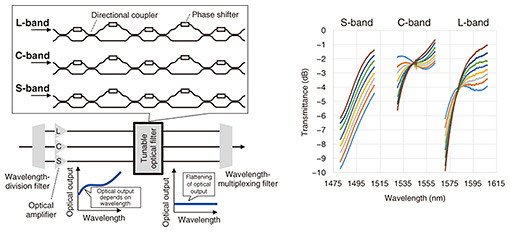
Feature Articles: Frontlines of IOWN Development—Development of IOWN Hardware and Software and Social Implementation Activities Vol. 23, No. 7, pp. 20–27, July 2025. https://doi.org/10.53829/ntr202507fa2 Development of Device Technology for IOWN ImplementationAbstractThis article introduces the development of device-related technologies at NTT Device Innovation Center. Such devices can be broadly divided into signal processing, computing, optical interconnect, and life-assist. We describe each of these devices and related initiatives. Keywords: IOWN, photonics-electronics convergence, data-centric infrastructure  1. Signal-processing devicesNTT Device Innovation Center has been conducting research and development on photonics-electronics signal-processing devices as the foundation for the All-Photonics Network (APN) in the Innovative Optical and Wireless Network (IOWN) promoted by NTT. Regarding photonics signal-processing devices, we have been developing and implementing optical switches, optical filters, and optical nodes, such as fan-in/fan-out devices for multi-core fiber using silica-based planar lightwave circuits (PLCs), toward large-scale and multiband implementation. Regarding electronics signal-processing devices, we have been developing and implementing a coherent digital signal processor (DSP) that will execute major digital signal processing in a digital-coherent optical-transmission system for large-capacity, long-distance, and low-power optical transmission. In this article, we describe PLC devices and a coherent DSP as signal-processing devices supporting a large-capacity optical network. 1.1 PLC devicesWe describe silica-based PLC devices that are widely used in large-capacity networks. Such devices have excellent optical performance, reliability, and manufacturability. Typical examples include arrayed waveguide gratings used as multiplexing/demultiplexing filters and multicast switches used in CDC-ROADM (colorless, directionless, contentionless reconfigurable optical add/drop multiplexing) systems. Multiband transmission technology for expanding wavelength bandwidth has been attracting attention for expanding network capacity, and on the basis of this trend, we are developing a tunable optical filter to compensate for wavelength dependence of optical-fiber loss and for power transitions between wavelength-multiplexed optical signals. The circuit configuration of this tunable optical filter is a cascade connection of multiple directional couplers via waveguide pairs with phase shifters having an appropriate path-length difference (Fig. 1 left). By adjusting the amount of phase shift, transmittance spectra having various types of smooth curves can be generated. As shown from examples of transmittance spectra settings (Fig. 1 right), this tunable optical filter can operate not only in the C-band*1 and L-band*2 communication-wavelength bands commonly used but also in the S-band*3 expected for use in the future [1]. Therefore, on the basis of trends in transmission technologies, such as expanding transmission-wavelength bands, we are working to achieve practical devices that can contribute to the implementation of high-speed and large-capacity optical nodes.
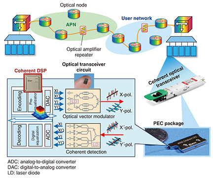
1.2 Coherent DSPWe describe a coherent DSP (Fig. 2) that will execute major signal processing in large-scale, digital-coherent optical transmission. A coherent DSP handles the polarization, amplitude, and phase of an optical signal as digital data and executes advanced signal processing to compensate for optical-signal distortion caused by optical-fiber transmission links and optical/electronic devices. This enables transmission capacity to be dramatically increased.
Digital-coherent optical transmission has increased transmission capacity from the conventional 100 Gbit/s to 1.2 Tbit/s per wavelength and modulation speed from 32 to 140 Gbaud. Remarkable progress has also been made in lowering power consumption to economically increase system-packaging density, and transmission energy per bit of an optical transceiver has been lowered from more than 500 pJ/bit to less than 40 pJ/bit, improving power efficiency by more than one order of magnitude. We have recently succeeded in developing a low-power coherent DSP that achieves a transmission capacity of 800 Gbit/s per wavelength at 25 pJ/bit. We also developed a photonics-electronics convergence (PEC) co-package that integrates optical devices and a coherent DSP. These devices can be implemented in compact transceiver modules such as QSFP-DD (quad small form factor pluggable double density) or OSFP (octal small form factor pluggable), enabling the implementation of a large-capacity optical-transmission system with low-power and high space density. We are developing a next-generation coherent DSP to achieve digital-coherent optical transmission over 1 Tbit/s in a more compact configuration with even less power consumption. We will work to develop practical PEC devices to increase the capacity and lower the power consumption of optical-transmission systems in datacenter networks and trunk networks such as the core/metro network.
2. Computing devicesWe aim to create and implement a computing architecture that can execute massive data processing without increasing environmental load. We describe our efforts in researching and developing a 51.2-Tbit/s large-capacity Ethernet switch (PEC switch, Fig. 3) equipped with PEC devices and an ultra-high-definition video artificial intelligence (AI)-inference large-scale integrated circuit (LSI) (Fig. 4) capable of executing low-power AI-inference processing in real time against 4K video.
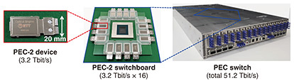
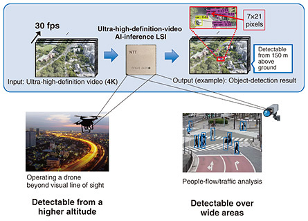
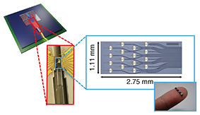
2.1 51.2-Tbit/s large-capacity Ethernet switch (PEC switch)At NTT, we have been developing PEC technology toward compact, large-capacity, and low-power devices through the integration of electronic and photonic circuits. As a first step in this effort, we developed a practical PEC device called PEC-1 that is mounted on a digital-coherent optical transceiver for use in optical-communications-network systems. We are now investigating its application to new architecture called disaggregated computing as the next stage in the deployment of this PEC device. This is new architecture that breaks away from the conventional central processing unit (CPU)-centric control limited to the server chassis. It is a concept to execute control by pooling together many computing resources, such as CPUs, graphics processing units, and field-programmable gate arrays, through optical connections. This architecture enables highly flexible resource control in rack scale and achieves high-performance computing while lowering power consumption [2]. In disaggregated computing, the interconnect function that connects each computing resource in a large-capacity, high-speed manner plays an important role. With this in mind, we prototyped a PEC switch equipped with PEC-2 devices to maximize the performance of this interconnect function. In this switch, 16 PEC-2 devices each having a bit rate of 3.2 Tbit/s are placed adjacent to each other around a switch LSI chip (electronic circuit), achieving a large-capacity switching function with a maximum bit rate of 51.2 Tbit/s. Note that the conventional Layer 2 switch featured a structure in which many pluggable-type optical transceivers were arranged on the front panel. Therefore, electrical wiring from the switch LSI to the front panel was somewhat long, leading to an increase in power consumption. However, since the structure of this prototype PEC switch places PEC devices near the switch LSI, power consumption originating in wiring can be minimized; thus, together with the power performance of individual PEC-2 devices, we have significantly reduced power compared with conventional switch equipment. Our plan is to use this PEC-2-mounted PEC switch to achieve large-capacity, low-power disaggregated computing that can make flexible use of computing resources. 2.2 Ultra-high-definition-video AI-inference LSIAI inference executed against video generally requires limits to the size of the input picture from the viewpoints of reducing computational complexity and simplifying training. Thus, even video of subjects shot with a commercial 4K camera, for example, must be reduced to a small picture size to execute AI inference. This process, however, can crush small objects making it difficult to detect them. Real-time characteristics and power consumption are also issues. NTT solved the above problems by establishing technology that enables the efficient execution of AI inference using 4K video as-is. This technology consists of two key technologies. The first is resolution-extension technology that extends the resolution limit of AI inference up to 4K video, and the other is NTT’s original AI-inference engine that enables real-time and low-power execution of that technology. To execute inference without reducing picture size, the resolution-extension technology divides the input picture size into smaller constrained size pictures and executes inference processing for each divided picture. This technology enables the detection of small objects. It can also reduce the entire picture then execute inference so that large objects that straddle those divided pictures can be detected. Final detection results can then be obtained by synthesizing the results obtained from the entire picture and those from the divided pictures. In short, this technology enables detection of both large and small objects in 4K video. This resolution-extension technology results in many divided pictures in 4K video, which can greatly increase computational complexity. Therefore, our original AI-inference engine uses, for example, inter-frame correlation to improve computational efficiency, which reduces computational complexity while preserving detection accuracy and enables 4K real-time execution with low power consumption. Mounting NTT’s ultra-high-definition-video AI-inference LSI equipped with this technology on edge devices, terminals, etc. and executing real-time AI inference against 4K video with a wide angle of view enables a variety of applications including the detection of desired objects, such as pedestrians or cars under a drone’s flight path from even higher altitudes, and desired objects from an even wider range in people-flow analysis. Using this LSI as a video-AI-inference accelerator for datacenters has the prospect of reducing power consumption in a variety of video-AI services using the cloud. 3. Optical-interconnect devicesA huge amount of data is exchanged daily on the communication network that supports our modern society, while capacity continues to grow resulting in an explosive increase in the power consumed by these processes. Reducing the power consumed in the communication system is a major objective with NTT’s IOWN, and establishing and implementing PEC technology is indispensable to meeting this objective. A key feature of optical-data transmissions is that power consumption does not easily increase even at high transmission speeds compared with electrical data transmissions. Current optical-data-transmission technology has been used for communications over relatively long distances, as in intercontinental communications, metro-access networks, and communications within datacenters. In contrast, electrical wiring is generally used for intra-board and inter-LSI connections and for intra-chip communications. IOWN, however, calls for the introduction of optical communications even in the short-range domain, such as intra-board and inter-LSI connections, using PEC technology. Our aim, therefore, is to greatly increase data-transmission speeds and reduce power consumption in all types of domains from network to computing. PEC-3, now under development, is an optical-interconnect technology between packages for LSI and other logic circuits. Only electrical wiring is currently being used for signal input/output with LSIs, but to make these connections faster with low power consumption, we are developing devices called optical chiplets for PEC-3 devices that interconnect LSIs through an opto-electronic conversion module. The key technology for interconnecting LSIs at high speeds and high densities with low power consumption is the membrane device. The term “membrane” refers to a thin film, and such a device has a structure in which a thin-film optical-functional element consisting of an indium phosphide (InP) compound semiconductor with a thickness of 200–400 nm is fabricated on a silicon (Si)-based large-scale optical circuit. Silicon, which is widely used in electronic circuits and elsewhere, enables the use of advanced microfabrication technology that enables the development of low-loss and large-scale optical circuits called Si photonics. However, it is difficult to fabricate light-emitting devices with Si photonics. In contrast, InP-based compound semiconductors, which are used in semiconductor lasers and other devices in optical communications, excel at generating light and optical-signal modulation. In short, the membrane device is NTT’s original heterogeneous-material integration technology that leverages the strong points of these materials. Membrane devices use a structure in which current flows in the lateral direction of the semiconductor thin film, and we use a structure that confines the thin film in the vertical direction through insulation material with a low refractive index with respect to a SiO2 (silicon dioxide) semiconductor. Thus, light can be confined in an extremely small region about one-tenth that of conventional semiconductor lasers, enabling efficient optical amplification and optical absorption within the semiconductor and high-speed and extremely low-power operation. Regarding the development of PEC-3 using membrane devices, we are developing optical-functional elements that integrate diverse functional elements such as membrane lasers that generate light and electro-absorption modulators that execute optical modulation. An overview of an optical chiplet that integrates the membrane devices under development is shown in Fig. 5. Sixteen channels of membrane lasers are integrated on an extremely small Si photonics chip that can fit on a fingertip. Each channel of these membrane lasers can transmit high-speed signals over 100 Gbit/s. This optical semiconductor chip is mounted on an optical chiplet in a form laminated with an electric chip and is modularized as an optical transmitter by connecting to an optical fiber. Our main goals in the development of this PEC technology are to secure the long-term reliability of membrane devices and launch optical-chiplet mass-production technology as early as possible. We anticipate that this technology will be incorporated in IOWN 3.0 targeted for implementation in 2028.
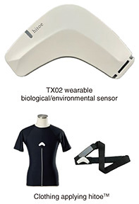
An optical chiplet is a technology that can connect LSI logic circuits at high speeds with low power consumption. Applying them widely to servers and computing systems will enable the optimal connection and processing of multiple resources (disaggregated computing). Although this technology is related to tiny semiconductor chips, the optical chiplet is essential technology supporting IOWN, which has the potential of transforming the world. With this in mind, we are conducting research and development to achieve the social implementation and spread of this technology as soon as possible. 4. Life-assist devicesWe are developing devices with the mission of contributing to a prosperous and sustainable society by extending the lifetime of both “people” as players in NTT’s IOWN and “infrastructure” as the foundation of IOWN. With regard to people, we are promoting medical-care and healthcare business in the NTT Group and developing wearable-device technology that can contribute to health management. Typical of this device development is the TX02: wearable biological/environmental sensor (Fig. 6) marketed by NTT TechnoCross. This sensor can be attached to hitoe™*4 clothing (such as shirts and belts) to automatically obtain biological information (electrocardiogram and heart rate) of the wearer, temperature and humidity within the wearer’s clothes, and acceleration. It incorporates a function for analyzing features, such as heart rate and number of steps, on the basis of measured data and enables transmission of analysis results to the wearer’s smartphone or an Internet-of-Things gateway via a wireless module so that real-time monitoring can be executed. In this regard, continuously conducting measurement, analysis, and communication by multiple sensors would normally shorten device operating time, making frequent charging and a large battery necessary. For TX02, we developed multi-sensor-data signal-processing technology that executes waveform processing and feature analysis in bulk by storing data in a buffer and running the CPU for only a short time through a function that pauses CPU operation. This technology enables continuous measurements of more than 40 hours with a small battery. The data obtained with TX02 can be used to manage the risk of a worker becoming sick due to heat exhaustion by estimating changes in internal body temperature and the risk of becoming unwell using a real-time estimation technique developed jointly with Nagoya Institute of Technology. This function is currently being provided by NTT TechnoCross as hitoe™ heat countermeasures service for Cloud [3]. We are thus involved in the development of not only wearable devices but also methods of using the data collected with these devices.
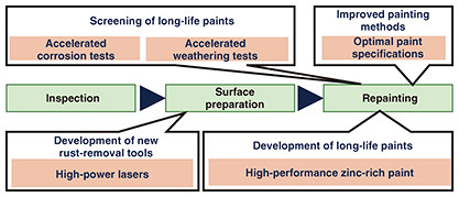
For infrastructure (which refers mainly to outdoor communication facilities), we are developing technology for analyzing the deterioration of materials used in such facilities to achieve long-life and extended-life facilities from the viewpoint of materials, and technology for increasing the efficiency of inspection and maintenance work through the use of developed devices as tools. We introduce an example of applying these technologies to the maintenance of steel towers used for communications. In such maintenance, one means of protecting the steel that serves as structural material is painting. Before painting, however, degraded coating and any rust on the surface of the steel must be removed, and the surface must be prepared, so maintenance consists of inspection, surface preparation, and repainting process (Fig. 7). For surface preparation, power tools and hand tools have traditionally been used, but in place of these, we are developing surface-preparation technology based on high-power lasers as tools that can remove salt with no reaction force with the prospect of automation. For painting, we are developing evaluation technology for screening long-life paint using accelerated corrosion testing and accelerated weathering testing. In addition to optimizing the method for applying multiple coats of paint (paint specifications), we are developing technology for improving the performance of zinc-rich paint (paint containing highly concentrated zinc powder). We are thus working to make steel-tower maintenance more efficient and lengthen the maintenance period (achieve long-life facilities).
References
|
|||||||||||||||