|
|||||||||
|
|
|||||||||
|
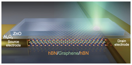
Front-line Researchers Vol. 23, No. 7, pp. 1–6, July 2025. https://doi.org/10.53829/ntr202507fr1  Pioneering the Understanding and Functional Exploration of Carrier Dynamics in Atomic-layer MaterialsAbstractMost active devices, such as transistors and photodetectors, currently used in information communications are based on semiconductors. Since the successful isolation of graphene in 2004, atomic-layer materials consisting of a single layer of atoms have attracted increasing attention. A variety of new materials have been discovered, along with novel phenomena and properties, paving the way for the development of next-generation devices that apply these unique properties. We spoke with Norio Kumada, a senior distinguished researcher at NTT Basic Research Laboratories, who is investigating the fundamental understanding and functional exploration of carrier dynamics in atomic-layer materials. We asked him about the results of his research, which aims to produce ultrafast devices by understanding the relationship between combinations of atomic-layer materials and their performance, as well as the enjoyment of the research process. Keywords: atomic-layer materials, graphene photodetector, graphene plasmon wave packet  Creation of the world’s fastest graphene photodetector and successful electrical generation, propagation control, and measurement of the world’s shortest graphene plasmon wave packet—Would you tell us about the research you are currently conducting? My research involves using so-called “atomic-layer materials” to read out ultrafast electrical signals and control those signals electrically. Specifically, I am investigating the theme of fundamental understanding and functional exploration of carrier dynamics in atomic-layer materials through on-chip terahertz (THz) current measurement. These atomic-layer materials are sheet-like materials consisting of a single layer of atoms, typically obtained by mechanically exfoliating one atomic layer from a bulk crystal. The most well-known example is graphene, which was first successfully isolated in 2004 by exfoliating a single atomic layer from graphite. This method of producing graphene earned two doctors from the University of Manchester in the UK the Nobel Prize in Physics in 2010. Since then, it has become possible to create atomic-layer materials with a variety of substances. Stacking different atomic-layer materials made it possible to create different materials with new properties; thus, atomic-layer materials became one of the emerging areas of interest in condensed matter physics and materials science. Since the fabrication process involves manually exfoliating and stacking monolayers, there are limitations in measurement techniques. Therefore, the full potential of atomic-layer materials has yet to be fully appreciated. As I mentioned above, atomic-layer materials have a very short history at the implementation level, and many aspects remain unknown. Under such circumstances, many researchers worldwide are taking on the challenge of analyzing these materials’ properties and pioneering their applications from their own standpoints. Conventional devices, such as semiconductor photodetectors, face inherent limitations in their operating speed due to electrical resistance and the detectable spectral range by the band gap. Regarding silicon photonics, device miniaturization is constrained by the diffraction limit of light. To develop new materials, physical phenomena, and control technologies that break through the limitations of conventional devices, we are measuring the behavior of electrons in atomic-layer materials on an ultrafast time scale—within one picosecond. By precisely measuring how electrons respond to incident light and how this response is converted into electrical signals, we aim to gain a deeper understanding of photodetector operation in atomic-layer materials. By analyzing the relationship between the combinations of atomic-layer materials and their resulting performance, we aim to propose novel device architectures capable of surpassing the constraints of current technologies. Demonstration of the potential of graphene as a broadband, high-speed photodetector material that will contribute to achieving ultrafast signal processing at THz frequencies—You recently announced two results, correct? Our two recent results were announced under the following press-release titles: (i) “Realizing zero-bias operation of a graphene photodetector at 220 GHz and elucidating the optical-to-electrical conversion process—Demonstrating the promise of graphene as a broadband high-speed photodetector material” (in collaboration with the National Institute for Materials Science (NIMS)) and (ii) “Electrical generation, propagation control, and detection of the ultrashort graphene plasmon wave packets—Contributing to the realization of ultrahigh-speed signal processing at terahertz frequency” (in collaboration with the University of Tokyo and NIMS). Regarding the result concerning a graphene photodetector, graphene has been theoretically shown to operate over an ultra-broadband of frequencies from THz waves to ultraviolet light and to exhibit high absorption efficiency, despite being only a single atomic-layer thick. However, the experimentally demonstrated operation speed under zero bias (that is, when no voltage is applied across the source and drain electrodes) has been limited to 70 GHz. This limitation arises from constraints in device structure and measurement equipment, preventing access to the intrinsic response of graphene. We therefore took on the following two challenges in regard to creating a broadband, high-speed photodetector using graphene: first, demonstrate an operating speed of 200 GHz (theoretical operating speed is over 200 GHz) and second, clarify the essential physical properties, such as the process by which optical signals are converted into electrical signals, of graphene. To address the two above-mentioned challenges, we fabricated a graphene photodetector (Fig. 1) on a sapphire substrate as follows. First, graphene is sandwiched between insulators, hexagonal boron nitride (hBN), provided by NIMS. Metal source and drain electrodes are then connected to each end of the hBN/graphene/hBN, the surface of which is then covered with an alumina (Al2O3) insulating film. Finally, a zinc-oxide (ZnO) gate is formed on top of the insulating film to avoid the current delay that occurs with conventional metal gates.
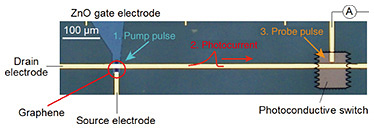
As shown as the three steps in Fig. 2, a pump pulse (a 280-fs laser pulse) generates a photocurrent. The photocurrent propagates along the drain electrode and is detected with a photoconductive switch irradiated with a probe pulse. The photocurrent waveform is measured by changing the time difference between the pump and probe pulses. The measurement results indicate the high-speed operation (220 GHz) of a graphene photodetector, consistent with its theoretically predicted performance. By comparing the characteristics of photodetectors with graphene of various quality, we revealed a trade-off between operating speed and sensitivity.
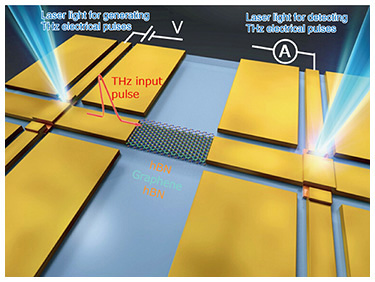
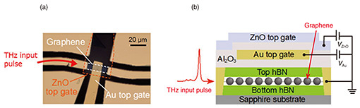
By analyzing these results, we explained the process by which graphene converts optical signal into an electrical one. In particular, contrary to previous common knowledge, we showed that the response time of the photocurrent is virtually independent of the size of the photodetector. We also showed that the current generation time after the pump pulse can be tuned from less than 100 fs to more than 4 ps by controlling the carrier density of graphene. These findings provide essential insights for designing graphene photodetectors tailored to specific applications such as information processing and sensing. The results were published in Nature Photonics on August 25, 2022 [1]. For future work, we plan to conduct similar on-chip photocurrent measurements on various atomic-layer materials in an attempt to increase the operating speed of the photodetector to 1 THz or more. —What is the other result? The THz region, which is promising for high-speed wireless communications, sensing, and imaging, has long been considered an unexplored area. However, a path toward social implementation as a use case for THz waves propagating in free space is emerging. In contrast, the technology for controlling THz electrical signals in circuits is still in its infancy, and the signal bandwidth that integrated circuits can handle is generally limited to the gigahertz band. We are focusing on the propagation control of graphene plasmons*1 as a new methodology to overcome this limitation and achieve faster signal processing. In our experiment, we generated and propagated graphene plasmon wave packets*2 by applying THz electrical pulses with a pulse width of 1.2 ps (Fig. 3). The amplitude and phase of the graphene plasmon wave packet was controlled with a metal gate. The conversion efficiency between the electrical pulse and plasmons was increased with a ZnO gate. By measuring the real-time waveforms with sub-picosecond time resolution, we evaluated the propagation characteristics, controllability, and plasmon-generation efficiency (Fig. 4).
The results of the above experiment clarified the following three points for the first time. (1) We succeeded in generating, controlling the propagation, and measuring an ultrashort (1.2 ps) graphene plasmon wave packet on a chip. We found the pulse width to be equivalent to the time width of the incident electrical pulse, making it the world’s shortest electrically excited plasmon wave packet. This result indicates that THz electrical signals can be transmitted without distortion. (2) We found that the phase and amplitude of the graphene plasmon wave packet can be controlled by electrically modulating the charge density of graphene via gate bias. Controlling the phase and amplitude is a fundamental operation in any type of signal processing. In other words, we demonstrated a new device operation for handling electrical signals in the THz range. (3) By optimizing the gate-electrode material, we achieved conversion efficiency of up to 35% from an electric pulse to a graphene plasmon wave packet. This value is several orders of magnitude higher than conventional light-to-plasmon conversion efficiency, indicating that graphene plasmons are inherently suitable for handling electric signals in the THz range. We also clarified that not only conversion efficiency but also the confinement effect, propagation speed, and pulse width depend on the gate-electrode material. These findings make it possible to optimize device structures according to purpose. The above research results were published in Nature Electronics on July 17, 2024 [2]. We plan to expand this work to applications in plasmonics (a technology for controlling wideband, high-speed signals in electronic circuits). From a different perspective, we also plan to explore applications in quantum-information processing. Specifically, we intend to pursue ultra-low-temperature THz measurements and the excitation of ultrashort single-electron pulses for flying electron qubits. This will pave the way for on-demand generation and distribution of entangled electron pairs.
We aim to be a front runner in the field by promoting our results that explain the detailed processes and mechanisms underlying the observed phenomena and ultimately lead to the discovery of optimal substances—What do you keep in mind as a researcher? In my current field of research, since the fabrication of graphene, not only have theories been verified but also a variety of new physical phenomena have been discovered. Atomic-layer materials other than graphene have appeared in a manner akin to a new world suddenly opening up. Each researcher has found their own research subject and is investigating it, so atomic-layer materials is a field in which anyone can aim to be a front runner. In this context, I’m pursuing research with the desire to demonstrate—by using different materials—performance that would never be achievable through the extension of refinements of current semiconductor devices and to publish the results of this research. In that sense, I’m aiming to be a front runner in my field of research. With that aim in mind, as a fundamental researcher, I’m conducting research with the belief that explaining the detailed mechanisms of the phenomena that occur during each process is important. For example, when a material is excited by light, the photoexcited electrons eventually return to their ground state by losing energy. Understanding how they interact with other particles during this relaxation process, and what kind of electrical signals are generated through what mechanisms, is key. I believe that unraveling these processes will ultimately lead to the discovery of optimal materials. With that conviction, I approach my research with a focus on generating meaningful results and actively communicating them to the broader community. Since there are relatively few groups using the same approach, it is important to appeal to a broader audience in a way that will interest them. Cutting-edge research often involves international collaboration, and at the entry stage, when team members are being selected and chosen, it is extremely important that they are interested in your research. For that reason, we have come up with various strategies to respond to this importance, since the location, timing, and presentation method, such as at academic conferences and international conferences, can all affect how interested participants are. Of course, it is most important to have results that you can highlight. Fortunately, as I mentioned above, the number of researchers in this specific research field is still small, and each of us is a front runner in our own narrow field, so we understand each other’s presentation content and have a mutual respect for it. We also share a common desire to get more people interested in our work, so I think that these challenges will be resolved by us competing with each other. In this situation, I have recently been able to participate in discussions as a partner in a European consortium fund, and because the impact of the two aforementioned results was significant, I am receiving more invites to lectures and other opportunities. I thus feel like things are gradually moving in a positive direction. Therefore, I want to take advantage of these opportunities to maintain this positive situation. Enjoy the research process—What is your message for younger researchers? Personally, I find the process of my research interesting and enjoyable, namely, seeing something no one has ever seen before, even if it is a small discovery, organizing it academically, announcing it to the outside world, and having it recognized by people worldwide. I am sure some researchers think in the same way as I do, while others are conducting research to achieve a certain goal, and I urge you to continue your research without forgetting that original intention. References
■Interviewee profileNorio Kumada received a B.S., M.S., and Ph.D. in physics from Tohoku University, Miyagi, in 1998, 2000, and 2003. He joined NTT Basic Research Laboratories in 2003. Since then, he has been engaged in the study of highly correlated electronic states confined in two dimensions. From 2013 to 2014, he was a visiting scientist at CEA Saclay, France. He received the Young Scientist Award of the Physical Society of Japan in 2008 and the Young Scientists’ Prize from the Minister of Education, Culture, Sports, Science and Technology in 2012. He is a member of the Physical Society of Japan. |
|||||||||