|
|
|
|
|
|
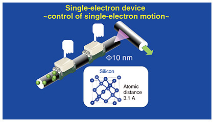
Rising Researchers Vol. 23, No. 7, pp. 7–12, July 2025. https://doi.org/10.53829/ntr202507ri1  Using Silicon Transistors to Enable Control and Detection of Single Electrons toward Developing High-performance Devices and Reducing Energy ConsumptionAbstractSemiconductors are used in many familiar electrical appliances such as televisions, personal computers, and smartphones. As a semiconductor device, a transistor plays important roles such as amplifying and switching electrical signals. Artificial intelligence (AI), which has been attracting much attention, requires high-speed processing, which is contributing to a dramatic improvement in semiconductor performance. However, the development of new technologies and services based on AI requires huge amounts of electricity, so new measures to reduce power consumption and ensure future sustainable development are necessary. We spoke with Katsuhiko Nishiguchi, a distinguished researcher at NTT Basic Research Laboratories who has created the world’s only transistor that can control a single electron at room temperature and is aiming to pioneer revolutionary technology to reduce the power consumption of semiconductors. Keywords: single-electron control, silicon transistor, nanodevice  The world’s only silicon device featuring “1 electron = 1 bit” technology—Would you tell us what kind of research you are conducting? We have all heard the word “semiconductor” on television or other media. Originally, “semiconductor” described the materials that make up the components (devices) that execute computations used primarily in televisions and smartphones. However, it has now become a word with such broad meaning that it has become a general term for components and an entire industry. Semiconductor devises are made up of a collection of switches called transistors that control the flow of electrons, and the general method of improving the performance of semiconductors is to pack many transistors as possible into the device (so-called integration) to increase its computing power. A smartphone, which is considered to be a cutting-edge technology, contains more than 19 billion transistors. However, the number of transistors cannot be increased using methods such as biotechnology, by which lactobacilli are cultivated in large quantities with the help of life force. Since transistors are made by highly artificial processes, such as cutting and heating substrates and thin films, it is extremely difficult to increase the number of integrations. Manufacturing costs are thus high, and building a fabrication plant requires an investment of hundreds of billions of yen, sometimes in the trillions of yen. Other major challenges must be overcome. Artificial intelligence (AI) is currently attracting much attention, and many people worldwide are using AI services. Behind the scenes, cutting-edge semiconductors are being used to enable AI to “learn.” Just one round of this learning consumes the same amount of electricity as generated by one nuclear power plant; in other words, in exchange for the advanced functionality of AI, an enormous amount of electricity is required. When a user searches for something by using AI, the answer is estimated from the results of the AI’s learning, and the electricity required for this process is said to be an order of magnitude greater than that of conventional search methods. To give you an everyday example, just one search by AI (information acquisition) on a smartphone consumes about one-third of the battery charge. While it is expected that various services and social developments using AI will continue to emerge, reducing the amount of power consumed by AI will be a major challenge. To solve the problem of the power consumption of AI, it is necessary to increase power generation and lower the power consumption of semiconductors. In the USA, to increase power generation, resumption of operations of the Three Mile Island Nuclear Power Plants (one of which has been shut down since the accident that occurred in 1979); use of smaller nuclear power plants; and use of renewable energy, such as solar power generation using vast areas of land, are being seriously considered. While it remains to be seen whether the same approaches are possible in Japan, power supply is an issue that cannot be avoided. Under these circumstances, it is becoming increasingly important to reduce the power consumption of semiconductors. Considering this importance, NTT is striving to reduce the power consumption of semiconductors by applying new principles. I mentioned above the importance of reducing power consumption of using AI services as an example, but new effects from dramatically reducing power consumption can also be expected. For example, semiconductors may not require batteries in the future and, instead, run on extremely small amounts of energy obtained from water or body heat. To actualize that future, we need a major breakthrough rather than just the further development of current technology; thus, we are conducting research that spans a long time (in the order of decades). Toward that breakthrough, we are creating single-electron devices in which a single electron operates as one “bit,” which is the unit of binary information used in computers and other devices. Each bit is usually represented as binary information “0” or “1” by using 100,000 or 1 million electrons. In other words, even if we use 1 million electrons, we can still only represent a single binary digit, “0” or “1,” with all those electrons. We are trying to reduce power consumption by representing 1 bit with a single electron instead of 1 million electrons in the conventional manner. Representing 1 bit with a single electron is very difficult, but a clever use of very small transistors makes it possible to represent 1 bit by moving a single electron and reading it out accurately. One example is a digital-to-analog converter (DAC) or pattern-recognition circuit that uses a single electron as 1 bit while consuming very little power. If the ability to readout a single electron is used as a sensor, it may be possible, for example, to identify ions in blood. Research on single electrons has generally required extremely low temperature environments, for example, minus 270°C. However, about 15 years ago, NTT’s unique proprietary technology became the first in the world capable of manipulating single electrons at room temperature, around 20°C (Fig. 1).
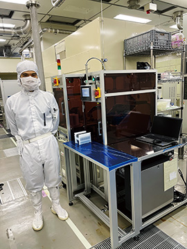
It is important to be able to operate in a room-temperature environment because it requires more electricity and energy to lower the temperature to minus 270°C, incurring costs. Current semiconductors will also not function properly in extremely low temperature environments, so new semiconductor-manufacturing technology that does not involve extremely low temperatures will be required. To manipulate a single electron at room temperature, the manipulating device must be made as small as a nanometer (one-millionth of a millimeter). As mentioned above, transistors are artificially created by machining materials and other processes, and NTT has long cultivated the technology to process transistors to such small sizes, so we can use those transistors to manipulate a single electron at room temperature ahead of the rest of the world. However, this possibility has revealed a problem related to processing precision. We fabricate devices using silicon, but at the nanometer scale, only a few dozen silicon atoms, the smallest unit of material, actually exist. Therefore, when processing a transistor, if we remove a few more atoms than the target, the characteristics of the device can change significantly. Although technology for processing accurately at the single-atom level is available, it cannot currently handle mass production of hundreds of millions of devices. Although we have succeeded in manipulating a single electron, for the above-described reasons, I believe that integrating single-electron devices will not be easy, even in the near future. However, 20 years ago, operation of single-electron devices at room temperature was thought to be extremely difficult, so I believe that our current achievement is significant in demonstrating the technological possibilities. The development of single-electron technology gave us the opportunity to find different perspectives on reducing the power consumption of semiconductors, and we realized that our devices were extremely important in proving these perspectives were valid. We are therefore now investigating reducing power consumption by taking a different approach. —Would you tell us about your research environment and research team? Transistors are fabricated using many different pieces of equipment and chemicals in a large clean room, in which the amount of dust and other contaminants is kept extremely low (Photo 1). It takes about six months to fabricate a transistor through a process that relies on a great deal of expertise and experience, and my fellow researchers and I do most of the work by hand, which I think makes us a rare group even within NTT laboratories. I believe that being able to use our accumulated experience, for example, when creating devices with new structures, differentiates us from other research groups.
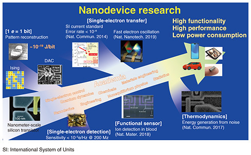
The fabricated devices are evaluated by using measurement instruments such as ammeters. In such evaluation, various methods are used to investigate whether the desired performance and whether any unexpected, unknown performance have been achieved. In this evaluation process, by understanding the most essential elements, such as the operating principle, it becomes possible to improve device performance and create and control new performance. To do this, it is important to use the academic and engineering knowledge accumulated by predecessors worldwide over decades and apply it to current technology. Among the most-recent semiconductor technologies, there are many examples of revivals of technology from several decades ago. While device evaluation poses different challenges from fabrication, it can also be said to be the “climax” when the results of a researcher become visible. —What are the unique strengths and characteristics of this research? A major advantage of our research is being able to create single-electron devices at room temperature, something that other researchers around the world have not been able to do yet. Another advantage is that we can now verify the ultimate operation of devices at room temperature on the basis of theories that were previously thought to be applicable at minus 270°C only. This ability is a significant advantage for us because it has made us realize that—while it is generally believed that single-electron devices can only be operated at extremely low temperatures—the highly versatile theories that become clear by operating the devices at room temperature are invaluable. Our single-electron device is an improvement over the silicon transistor. Silicon transistors bring together a variety of outstanding technologies and knowledge discovered by many companies, universities, research institutes, and other bodies, and semiconductor companies mature those technologies and turn them into products. Even if the technology and knowledge we have discovered are not enough to implement high-performance semiconductors, we can still contribute to society by incorporating them into semiconductors in the form of, for example, low-power-consumption technology. Although similar research on technologies that use superconducting materials and light is also being conducted, the use of silicon may be a major advantage of our research. Our aim is to theorize past research, obtain patents, and expand versatility—What are your future prospects and problems that need to be solved? Our goal is to reduce the power consumption of circuits and their elements, and we currently have the world’s only single-electron device, which is a major advantage. For the past three or four years, we have been using this device as a tool to find ways to reduce energy consumption from an academic perspective. The distance to our goal may seem far away, but I hope that the knowledge we have gained will become general-purpose knowledge enabling us to reach that goal. As I mentioned above, it will be difficult to integrate a number of single-electron devices from the perspective of processing accuracy; even so, I hope that if we can find a general-purpose technology that can be applied to general semiconductors, we may be able to reduce power consumption without having to worry about issues with processing accuracy. In the theoretical field we are working within, hundreds of papers are published annually, but only a few each year use expressions from the semiconductor and device field, our specialty. Although theoretical papers are supposed to provide basic, general-purpose theories, which can be applied to semiconductors, I feel it is difficult to apply these theories to semiconductors; in other words, it is like suddenly being spoken to in another language, even though I only understand Japanese. Helping me to face this difficulty is cooperating with other group members; some members are good at reading and understanding theoretical papers, while others have different points of interest in the same paper. I believe that these differences stem from our different past research activities, including our studies in our university days. I feel that the results we obtain are enhanced by the successful intertwining of these individual strengths. I am now the group leader, but when I write papers and present them at conferences, I still receive help from my group’s members who are good at the theoretical aspects, which I still lack experience in. I also receive advice from members on how to enhance the value of the results that I want to publish. Only recently have we finally begun to see ways to apply these published theories to semiconductors, and we are seeing results. However, we are still not close to the world we are looking for, and we need to overcome a number of hurdles. I believe that if we can overcome these hurdles, our research results will have a major ripple effect on the semiconductor industry (Fig. 2).
—What is your message to researchers and students? Students from universities in France, Canada, and the United States come to our laboratories on internships and join our research. Although these overseas students are not originally skilled in the field, they produce results that are sufficient for publishing in a paper in about six months. One of them has even won an academic-paper award. These students have thus become valuable assets. In contrast, as a lecturer at a university, I have noticed that although the students that I lecture know how to solve equations and other things, compared with our internship students, their problem-solving skills are lacking to an extent that concerns me. The difference between overseas students and Japanese students is that, for example, when the former begins a research project, they seem to make a strong effort to understand the value and essence of the research thoroughly. Even if the research topic is not their area of expertise, if they don’t understand something, they will study it and try to understand it. Therefore, when they begin actual research, they will be able to think independently about what they need to do, and when they encounter a problem, they can think of ways to solve it. If you do not have a firm understanding of the value and nature of your research, you will not be able to work independently. I feel that some Japanese students seem to be attending classes just to get credits, while other students blame the poor quality of the classes for their lack of interest. However, I believe that university is a place to acquire knowledge and think about things; accordingly, regardless of whether you are interested in the class’s topic, you need to have a challenging class that requires you to spend a month frantically researching and thinking about a topic and working on a report. I hope all students will keep my advice in mind and think of their important university years as precious time to study hard and think things through. Today, it is vital to advance your career to be able to succeed no matter which company you work for, and you will be able to carve your own path without being confined to the framework of a particular company. I want students to remember that to achieve that success, how they spend their university life is important. —What is your message to your business partners? Some people maybe didn’t know that ten years ago, we developed technology for moving a single electron. I regret that we didn’t promote that technology enough. If we had been able to promote the fact that single-electron technology exists to people in various fields at academic conferences and other events, the versatility of the technology would have increased as a result. Looking at industry trends, we see that the importance of design when making things, which is what we do, is undoubtedly increasing. We want to be able to theorize and release the knowledge we have thus gained in the form of intellectual property, patents, etc., so we are currently working within the theoretical field. We will also prepare manufacturing processes and methods, etc., so that our knowledge can be used in practice. We hope that our knowledge will be useful in your research and development. ■Interviewee profileKatsuhiko Nishiguchi completed his doctoral studies at the Department of Electronic and Physical Engineering, the Tokyo Institute of Technology (currently, Institute of Science Tokyo) in 2002. In the same year, he joined NTT. He has been engaged in research into nanostructured silicon devices aimed at reducing power consumption and enhancing functionality. In 2008, he was a visiting researcher at the French National Center for Scientific Research. From 2012 to 2013, he was a visiting researcher at Delft University of Technology (Netherlands). In 2015, he was a visiting associate professor at the Tokyo Institute of Technology. He is currently a distinguished researcher and Nanodevice Research Group Leader of Advanced Applied Physical Science Laboratory at NTT Basic Research Laboratories. In 2013, he received the Minister of Education, Culture, Sports, Science and Technology’s Young Scientists’ Award in the field of science and technology. |