|
|||
|
|
|||
|
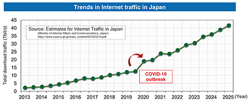
Rising Researchers Vol. 24, No. 4, pp. 8–13, Apr. 2026. https://doi.org/10.53829/ntr202604ri1  Ultra-wideband Analog ICs Using InP Semiconductors to Overcome the Limits of Optical CommunicationsAbstractAdvances in the communication environment, which supports the increasing volume of communication traffic, have been driven by improvements in digital signal processing and the performance of integrated circuits (ICs). However, it has become apparent that limitations in hardware performance are making fundamental improvements in bandwidth and speed increasingly difficult. Ultra-wideband analog ICs can provide a breakthrough in overcoming these limitations. This new technology makes it possible to move away from the conventional method of relying solely on the continued scaling of silicon-based semiconductors. In this article, we spoke with Munehiko Nagatani, a distinguished researcher at NTT Device Technology Laboratories and a leader in the field of ultra-wideband analog ICs. Keywords: analog IC, AMUX, ADEMUX, InP HBT  Ultra-wideband analog ICs will be the key to the development of optical communications and pave the way to the future—What prompted you to start researching ultra-wideband analog ICs, and what is the background to the demand for this technology? Driven by the spread and expansion of high-definition video streaming, global communication traffic is steadily increasing. The COVID-19 pandemic led to a rapid increase in demand for remote work and online meetings, and coupled with the spread of generative AI (artificial intelligence), this increase in communication traffic is expected to continue (Fig. 1).
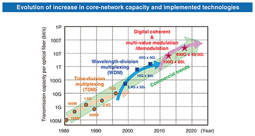
To address ever-increasing communication traffic, various technologies have been developed to expand transmission capacity of optical communication systems. For example, a new technology known as digital coherent technology* was commercially introduced between 2012 and 2013. Along with advances in the scaling of silicon-based semiconductors, the performance of large-scale digital signal processors (DSPs), digital-to-analog converters (DACs), and analog-to-digital converters (ADCs) has improved. Optical communication, which initially had a transmission capacity of 100 Gbit/s per wavelength, has now surpassed 400 Gbit/s and reached 800 Gbit/s (Fig. 2).
The expansion of transmission capacity largely depends on improvements in the performance of integrated circuits (ICs) such as the aforementioned DSPs, DACs, and ADCs; however, it has become a concern that the physical limits of miniaturization and speed improvements in these semiconductors are being reached. The technology node currently used for silicon-based semiconductors is said to be 3 nm, and as widely reported in the news, technological development toward mass production of the 2-nm node is gaining momentum. While such scaling is expected to increase integration density and improve the signal-processing efficiency of ICs, improvements in speed remain limited, and it is particularly difficult to achieve fundamental improvements in bandwidth (speed performance) for ICs such as DACs and ADCs. To accommodate future increases in transmission capacity, a new approach, one that does not rely solely on the continued scaling of silicon-based semiconductors, is therefore required. After joining NTT in 2007, I was assigned to NTT Photonics Laboratories, where I was involved in research and development of high-speed analog ICs for optical communications, particularly amplifiers and ADCs for receivers. Since then, I’ve also been involved in research and development of amplifiers and DACs on the transmitter side. Around 2014, based on this experience and knowledge, I began analyzing the fundamental hardware performance limits of these circuits and researching new analog IC technology to overcome these limitations. I’m currently developing this ultra-wideband analog IC technology in the form of analog-multiplexer (AMUX) circuits and analog-demultiplexer (ADEMUX) circuits.
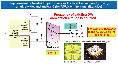
—Why do we need analog technology to increase digital communication capacity? Digital signal processing is a system that processes signals using a combination of 0s and 1s. In the early era of optical communications, signals were sent by switching lasers on and off in combination. However, this system is inefficient, so technology that makes it possible to send signals even in an intermediate state between “on” (1) and “off” (0) has been developed. The concept behind this technology is easier to understand by using the example of the brightness of a light bulb; that is, in addition to being either at its brightest or completely off, a light bulb can also be turned on at a lower brightness. Current digital coherent optical communication technology makes it possible to send signals at different brightness intensities, such as 0.8, 0.6, or 0.4. (Strictly speaking, information is carried not only as the intensity of the light but also as the phase and polarization of the light wave.) To put the signal into this intermediate state that is neither 0 nor 1, it is necessary to convert the digital signal into an analog signal (i.e., a multi-value signal). This conversion is done using a DAC on the transmitting side. An ADC on the receiving side then converts the transmitted analog signal back into a digital signal. It has thus become possible to send information in an intermediate state that is neither 0 nor 1 in a manner that has dramatically increased transmission capacity. In my research, I aim to increase transmission capacity dramatically by adding an ultra-wideband analog IC (equipped with multiple functions such as frequency conversion) to the DAC and ADC units of the digital signal processing system. —Please tell us about ultra-wideband analog IC technology. The ultra-wideband analog IC that I am proposing includes two ICs: an AMUX on the transmitting side and an ADEMUX on the receiving side. These ICs combine functional blocks such as an amplifier (for amplification), mixer (for frequency conversion), and combiner (for multiplexing). Using these ICs in combination with conventional DACs and ADCs makes it possible to eliminate the limiting factors (in terms of bandwidth performance) of conventional optical transmitters and optical receivers and overcome their limitations (Fig. 3).
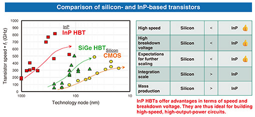
While current general-purpose ICs are mainly based on silicon complementary metal-oxide semiconductor (CMOS) technology, in 2019, NTT introduced an IC that uses a high-speed transistor technology called an indium-phosphide heterojunction bipolar transistor (InP HBT), which we had been researching and developing for many years. Although compared with silicon-based semiconductors, InP-based semiconductors have disadvantages concerning, for example, integration scale (multi-functionality) and mass production, they offer remarkable improvements in speed and breakdown voltage (Fig. 4). Accordingly, by using InP-based semiconductors, we have achieved the world’s first AMUX and ADEMUX circuits with 110-GHz bandwidth.
Since then, in collaboration with NTT Network Innovation Laboratories, we have demonstrated long-distance optical transmission exceeding 1 Tbit/s per wavelength and demonstrated unprecedented 200-GHz bandwidth performance. We also succeeded in optical transmission of 2 Tbit/s per wavelength, setting a new world record. We are currently working on commercializing and putting these ultra-wideband analog ICs into practical use for high-end measurement and experimental applications. However, rather than resting on our laurels, we want to develop this technology while aiming to achieve 300 GHz within 10 years. —Please tell us about any difficulties you faced in your research and any challenges you face in your future research. AMUX and ADEMUX circuits are completely new analog ICs with unprecedented functionality. Therefore, when incorporating them into an optical communication system, we had to proceed by trial and error without a clear understanding of the required performance levels. We then incorporated the completed prototype circuits in optical communication systems for transmission experiments and obtained feedback from the results of the experiments. Through repeated trial and error, we were able to determine the necessary wide-ranging circuit characteristics and continued to improve the circuits through repeated prototyping. I should add that applying each prototype in experiments did not happen overnight. Even if the core circuit of an IC is completed, the IC cannot be used in experiments—and users cannot use it—unless it is packaged and made into a module that can be connected to other devices via coaxial cables or the like. Obviously, low-loss, high-frequency packages capable of housing ICs with such unprecedented bandwidth performance were not available, so it took us several years to create a new, dedicated high-frequency package. In addition to these technical aspects, commercializing this new analog IC technology at a group company also required repeated dialogue with potential users, from the early stages of research and development, to determine the appropriate application areas. Moreover, what I can do alone is limited, so it was important to share the goal of commercialization with the people around me and get their cooperation. I’m grateful to everyone who worked tirelessly with me even when the product was still in its infancy. I don’t think we would have made it this far without a single person who has been involved in this research and development. The goal of our research team at NTT Device Technology Laboratories is to “support the sustainable development of communications,” so we intend to continue research and development and refine our technology so that it can be implemented in a timely manner when it is truly needed for communications. Technically, we plan to further expand the bandwidth (to over 200 GHz) and integrate functions while refining the technology to make it more compatible with optical transceivers, which have strict restrictions on both power and size. In terms of practical implementation, improving manufacturability and mass production is key for communications applications that must handle large volumes of demand, so we need to increase the number of partners willing to cooperate with us. Expanding into optical quantum computing and entering a new world of applications—Please tell us about what this technology can achieve and its applications. The main application of ultra-wideband analog ICs is currently optical communications; however, we have already begun putting this technology to practical use in high-end research and development experiments and the measurement field. Even at this stage, the potential needs for this technology are wide ranging, and we are considering expanding it into other fields that handle wideband signals (e.g., wireless communications and sensing). Since this technology may be in demand in the field of optical quantum computing, which NTT has been focusing on, we hope to take it beyond communications and explore new applications in the future. NTT’s Innovative Optical and Wireless Network (IOWN) initiative necessitates increasing capacity of optical communication systems beyond what is currently possible. Ultra-wideband analog IC technology can be used as one means to increase transmission capacity. The world envisioned with IOWN is based on photonics-electronics convergence technology, which aims to replace electrical wiring with optical wiring even for short-distance connections, which are currently dominated by electrical wiring. However, since a performance gap between broadband optical devices and bandwidth-limited electronic devices inevitably exists, we believe there is room for improvement in the efficiency of electrical-to-optical conversion. Our ultra-wideband analog IC technology developed via the above-described research should be able to contribute significantly to improving the efficiency of this electrical-to-optical conversion. —What are the principles or values that you consider important when conducting research? When conducting research and development, I am always conscious of taking on the challenge of doing something that no one else has done or has been able to do. In other words, I try to be enterprising and bold. However, to avoid being self-satisfied, I have pursued my research by understanding and analyzing currently used technologies and their trends, identifying problems and potential issues that no one has yet noticed, and deriving new solutions. When I act, I’m decisive and bold. I’d like to continue working in a way that creates new trends, rather than just following them. —Please tell us about NTT Device Technology Laboratories, where you work. NTT Device Technology Laboratories conducts research and development to create competitive device technologies that will bring about new developments and significant impact in business and society. For example, we aim to create surprising new technologies in the fields of photonics, electronics, materials science, and bioscience. NTT laboratories have a practical training system implemented company-wide. While the first year with the company is a period of basic training as a researcher, from the second year onward, one will develop their own research topic then independently pursue research under the guidance of a mentor (a senior employee with 10 to 15 years of experience) and several advisors (experts in each research field). In the third year, one is required to present their research progress and results in front of hundreds of fellow researchers. This training system enables one to learn—in concrete terms—how to initiate and advance research, how to set goals, and how to approach them. Researchers, including myself, are also encouraged to pursue a doctorate degree after joining the company. Obtaining a doctorate degree significantly changes how one is treated, particularly at overseas academic conferences, so I believe obtaining one is an effective measure to enhance one’s career. By thoroughly implementing this training system, we continue to produce many professional researchers who can be successful both in Japan and overseas.
—What is your message to researchers, students, and business partners? I joined NTT in 2007, so I have been working as a researcher for nearly 20 years. In this interview, I’ve talked about research themes that are currently progressing smoothly; however, I have also had the experience of failing to move from research to development and practical application and being forced to give up halfway through. At that time, I abandoned the research for various reasons, but I now understand and regret that one of the reasons was that I was unable to comprehend the changes in social needs between the time the research started and when it was abandoned. As I have experienced, research is never self-contained. It is important to translate research results into tangible value for society, and this task requires discussion and cooperation with others, including collaborators and potential users. It is essential to understand what is required at any given time and update your understanding as the times change. I’ve also made use of my past reflections, and in my current research, I consciously consider objectively the value of my current research and who my current efforts will benefit by discussing these matters with others and reconsidering how I’m proceeding. NTT has many researchers who are active at the forefront of a wide range of technical fields. We also have an environment in which we can proactively work on everything from research to practical application. The words of our first director, Goro Yoshida, spoken in 1950, “Do research by drawing from the fountain of knowledge and provide specific benefits to society through commercial development,” truly show us the direction we should take. I want to continue exchanging opinions with you all and push forward with research and development in a manner that provides specific benefits to society. Finally, the one thing I want to say to the next generation is to be bold, enterprising, and willing to take on new challenges without hesitation. In that way, you can make important discoveries while doing things that no one has done before. ■Interviewee profileIn 2005, during his third year at the Faculty of Science and Technology at Sophia University, Munehiko Nagatani skipped a year and advanced to the Graduate School of Science and Engineering. He completed his master’s degree in 2007. That same year, he joined Nippon Telegraph and Telephone Corporation. After working at NTT Photonics Laboratories and NTT Device Innovation Center, he joined NTT Device Technology Laboratories and NTT Network Innovation Laboratories. He is engaged in research and development of ultra-high-speed analog ICs. He received his Ph.D. in Engineering from Sophia University in 2021. He received the Minister of Education, Culture, Sports, Science and Technology’s Young Scientist’s Award and the Maejima Hisoka Encouragement Award in 2022, and the IEEE Tatsuo Itoh Award and the IEICE Electronics Society Award in 2025. |
|||