|
|||||||||||||||||||||||||
|
|
|||||||||||||||||||||||||
|
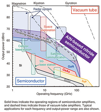
Feature Articles: Forefront Research on Ultrawide-bandgap Semiconductors Vol. 24, No. 6, pp. 27–33, June 2026. https://doi.org/10.53829/ntr202606fa3 High-frequency Operation of AlN-based Polarization-doped TransistorsAbstractAluminum nitride (AlN)-based nitride semiconductors exhibit an extremely high critical electric field and promising materials for the high-power and high-frequency devices required in next-generation wireless communications. However, in the high-Al-composition region, conventional impurity doping cannot provide sufficiently high carrier concentrations, which has hindered high-frequency transistor operation. We present polarization doping, a novel conductivity control technique that uses the polarization properties of nitride semiconductors, and introduce our latest research demonstrating the high-frequency operation of AlN-based transistors enabled with this technique. Keywords: aluminum nitride, high-frequency power amplifier, polarization doping  1. IntroductionAn enormous range of services and devices are connected to the Internet. Network connectivity now supports not only messaging and information search but also entertainment, financial services, and online commerce. Therefore, information and communication technologies have become indispensable to modern society. Information is exchanged through communication networks, either through wired networks using optical fibers or through wireless networks using radio waves*1. In wireless communications, the deployment of 5G (the fifth-generation mobile communication system) began in 2019, and the amount of data exchanged by mobile terminals has increased exponentially since then. By the 2030s, it is expected to reach approximately twice the current level (as of 2025). To support society and industry beyond 2030, research targeting the further advancement of wireless mobile communication systems, known as Beyond 5G, is currently underway. Beyond 5G is expected to provide communication services not only on land but also in the air, at sea, and in space. Therefore, expanding network coverage to areas beyond the reach of conventional terrestrial wireless networks has become an important challenge. To address this issue, non-terrestrial networks (NTNs), which use geostationary orbit satellites, low-Earth orbit (LEO) satellites, and high-altitude platform stations, are attracting increasing attention as a means of constructing communication networks across land, sea, air, and space. In NTN systems, long-distance wireless transmission technology is essential. However, radio waves attenuate with distance due to propagation loss. Therefore, high-power amplifiers operating at high frequencies are key components for NTN systems. Figure 1 compares the operating frequency and output power of semiconductor amplifiers and vacuum tube amplifiers. High-electron-mobility transistors (HEMTs)*2 based on gallium nitride (GaN) exhibit excellent performance as high-power semiconductor amplifiers and are widely used in base stations for mobile communications and as power amplifiers for transmission in some LEO satellites. For satellite communication applications requiring even higher output power, however, vacuum tube amplifiers (such as traveling-wave tube amplifiers) are still widely used. Such amplifiers have several drawbacks, including large size, limited lifetime, and vulnerability to mechanical shock. Therefore, developing ultrahigh-power and high-frequency semiconductor power amplifiers surpassing GaN-based HEMTs would enable the replacement of conventional vacuum tube devices, leading to power-amplifier miniaturization and longer device lifetime. This would ultimately contribute to the construction of more robust wireless communication networks.
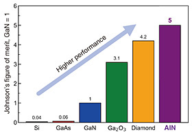
2. Expectation for AlN-based nitride semiconductorsFor high-power high-frequency semiconductor amplifiers, transistors capable of operating at high frequencies and withstanding high voltages are required. Therefore, semiconductor materials with both high critical electric field*3 and high electron saturation velocity*4 are desirable. We focus on aluminum nitride (AlN)-based nitride semiconductors as materials for enabling ultrahigh-power operation in high-frequency power amplifiers beyond the limits of conventional semiconductor materials. Specifically, AlN-based nitride semiconductors refer to AlN and AlGaN alloys with an Al composition greater than 50%. Among semiconductor materials, AlN exhibits the highest critical electric field—at least 7 MV/cm and an expected value as high as 12 MV/cm. It also has a high electron saturation velocity of approximately 107 cm/s. Therefore, AlN’s Johnson’s figure of merit, an indicator of the performance of high-power high-frequency transistors, is among the highest of all semiconductor materials, as shown in Fig. 2.
Compared with silicon (Si) or gallium arsenide (GaAs), the performance of AlN is several orders of magnitude higher, and even compared with GaN, an approximately five times higher performance is expected. In other words, we can expect an output power approximately five times higher than that of GaN at the same operating frequency. These properties make AlN a highly promising material for high-power, high-frequency devices. However, conductivity control in AlN-based nitride semiconductors remains a significant challenge. When the Al composition of the channel layer, which serves as the current path in a transistor, is increased, the channel resistance increases. For this reason, high-frequency operation of AlN-based transistors with an Al composition exceeding 75% has not been reported. To address this issue, we focused on an AlN-based polarization-doped field-effect transistor (pol-FET) that uses polarization doping, a conductivity control technique different from conventional impurity doping. Using this technique, we achieved a low-resistance channel layer even in high-Al-composition AlGaN and successfully demonstrated high-frequency operation of AlN-based transistors [1].
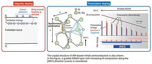
3. Polarization doping in AlN-based nitride semiconductorsIn semiconductor materials, the concentration of carriers, i.e., the electrons (negative charge) and holes (positive charge) that carry the electric current, must be controlled over a very wide range and with high precision depending on the application. This control is achieved by impurity doping, in which specific elements are introduced into the semiconductor crystal. For power devices that operate under high voltage, carrier concentrations in the range of 1014–1016 cm−3 are required. For high-frequency devices, such as those discussed in this article, carrier concentrations exceeding 1018 cm−3 are required. Impurities are not electrically active by themselves, and a certain amount of thermal energy is required to generate carriers. This threshold is called the ionization energy. In Si it is about 50 meV, and in GaAs it ranges from a few meV to about 30 meV, which is comparable to the thermal energy at room temperature (25°C), i.e., 25.7 meV. In Si and GaAs, therefore, the impurities are sufficiently ionized, and the carrier concentration is almost the same as the impurity concentration. In AlN-based nitride semiconductors, however, the ionization energy exceeds 100 meV in the high-Al-composition region, and most impurities are not ionized at room temperature (Fig. 3). For example, in n-type AlN, even when impurities are doped at a concentration of 1018 cm−3, the generated carrier concentration is only about 0.1%, approximately 1015 cm−3. Due to the low carrier concentration attributed to the large ionization energy, the formation of the low-resistance transistor structure is difficult, which has prevented the high-frequency operation of AlN-based transistors.
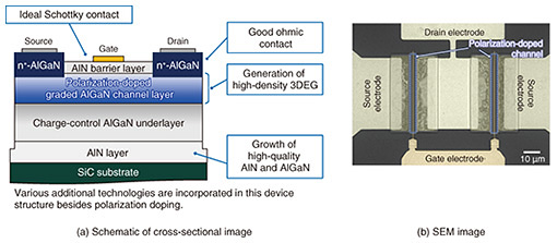
We therefore use polarization doping, which does not rely on conventional impurity doping. Group-III nitride semiconductors, such as AlN and GaN, exhibit ionic bonding due to the strong electronegativity of nitrogen (N) atoms. Thus, group-III atoms, such as Al and Ga, are positively charged and N atoms are negatively charged in the crystal. As shown in Fig. 3, group-III atoms and N atoms are arranged in a tetrahedral structure. However, the ratio of the lattice constants (c/a in Fig. 3) ranges from 1.626 to 1.601, which deviates from 1.633 for a regular tetrahedron. Therefore, the electric dipole moments due to ionic bonding are not completely canceled, resulting in a charge imbalance known as spontaneous polarization within the crystal. When semiconductor layers with different lattice constants are stacked, such as an AlGaN layer on GaN or an AlGaN layer on AlN, the upper layer is affected by the underlayer and tensile or compressive stress is induced. This strain further distorts the crystal structure and induces additional polarization, known as piezoelectric polarization. Polarization doping uses such polarization effects [2]. Figure 3 shows a schematic of n-type conductivity control in AlGaN by polarization doping. We consider a graded AlGaN layer in which the Al composition increases along the [0001] direction (c-axis direction). The polarization in AlGaN increases as the Al composition increases because AlN has a larger polarization than GaN. Therefore, a difference in polarization occurs between neighboring unit cells, and this difference extends throughout the graded AlGaN layer. In this case, the positive polarization charge is larger than the negative polarization charge of neighboring unit cells. Therefore, net positive charge corresponding to the difference is distributed within the graded AlGaN layer. However, this positive charge is a fixed charge that cannot move freely in the semiconductor crystal, thus does not contribute to electrical conduction. This is because the polarization charge is tied to the atoms that constitute the semiconductor crystal. A semiconductor, however, must maintain electrical neutrality, where positive and negative charges are balanced. Therefore, electrons with negative charge are induced in the graded AlGaN layer to balance this positive fixed charge. Electrons uniformly distributed throughout the graded AlGaN layer in three dimensions are called a three-dimensional electron gas (3DEG) and can move freely within the semiconductor crystal. Therefore, they contribute to electrical conduction, and this graded AlGaN layer exhibits n-type conductivity. The 3DEG concentration can be easily and precisely controlled by the composition gradient, that is, the difference in composition (difference in polarization) and the film thickness. Thanks to this process, polarization doping does not require impurities for generating carriers, and carrier densities exceeding 1018 cm−3 can be obtained even in AlN-based nitride semiconductors with high-Al composition. Thus, polarization doping is an important technique for AlN-based nitride semiconductor devices. 4. Polarization-doped FETs with AlN-based nitride semiconductorsFigure 4 shows the device structure of the fabricated AlN-based pol-FET with a polarization-doped AlGaN channel layer along with its scanning electron microscope (SEM) image. The structure was grown on a silicon carbide (SiC) substrate by metal–organic vapor phase epitaxy (MOVPE)*5. In this structure, a charge-control AlGaN underlayer is formed beneath the channel layer, and an AlN barrier layer is formed above it to maximize the generation of the 3DEG by polarization doping [3]. The charge-control AlGaN underlayer mitigates the influence of undesired fixed charges outside the channel layer, while the AlN barrier layer prevents surface exposure of the channel layer.
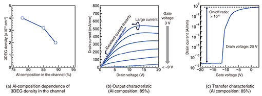
The 3DEG concentration in the polarization-doped AlGaN channel layer estimated from capacitance–voltage measurement is shown in Fig. 5(a). Even at very high Al compositions exceeding 75%, a high-density 3DEG of 2–4 × 1018 cm−3 is achieved, resulting in a low-resistance channel enabled by polarization doping. In addition to the polarization-doped channel structure described above, which enables the formation of a high-density 3DEG, this device also incorporates several proprietary technologies developed by our group: (1) high-quality growth technology for AlN-based nitride semiconductors, (2) ohmic contact technology that enables efficient current injection from the electrodes into the channel, and (3) ideal Schottky contact technology for controlling the injected current [4–6]. Figure 5(b) shows the current–voltage characteristics (output characteristics) of the fabricated AlN-based pol-FET with an Al composition of 85% in the channel. Due to these technologies, even in an AlGaN channel with a high Al composition of 85%, excellent current linearity in the linear region and a large drain current exceeding 500 mA/mm were achieved. Note that a transistor is required to not only conduct a large current but also turn it off by applying a gate voltage. As shown in Fig. 5(c), the fabricated AlN-based pol-FET exhibits excellent transfer characteristics with negligible leakage current, achieving an on/off ratio greater than 1010. This high on/off ratio is beneficial for high-frequency operation.
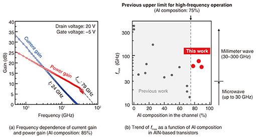
Figure 6(a) shows the high-frequency characteristics. For high-frequency amplifiers, the maximum oscillation frequency (fmax)*6 is an important performance indicator. The fabricated AlN-based pol-FET achieved an fmax of 79 GHz in the millimeter-wave band. As shown in Fig. 6(b), power amplification operation of a high-frequency transistor with an AlGaN channel having a high Al composition exceeding 75%, which had previously been difficult to achieve, was demonstrated for the first time at a practical frequency band. The fmax achieved in this study is the highest reported thus far for AlN-based high-frequency transistors. Therefore, the structure of the fabricated AlN-based pol-FET provides a key design guideline for unlocking the high potential inherent in AlN-based nitride semiconductors and represents an important step forward in the application of high-power high-frequency AlN-based transistors.
Even at a higher Al composition of 89%, power amplification operation with an fmax of 61 GHz was achieved. The bandgap energy of AlGaN with an Al composition of 89% is approximately 5.6 eV, which is the largest among semiconductor materials demonstrating high-frequency power amplification. These results also indicate that AlN-based pol-FETs are promising as ultrawide-bandgap semiconductor high-frequency amplifiers that can potentially achieve higher output power than conventional devices.
5. Future prospectsWe introduced high-frequency transistors based on AlN-based nitride semiconductors. By using polarization doping, we demonstrated that large-current operation and high-frequency operation are possible even in the high-Al-composition region. For future work, we will further improve and propose device structures to simultaneously achieve high-voltage operation. By unlocking the full potential of AlN-based nitride semiconductors, we aim to achieve high-power operation that surpasses conventional semiconductor devices. High-power high-frequency amplifiers are used not only in communications but also in a wide range of fields such as radar and space exploration. Therefore, AlN-based high-frequency transistors are expected to play important roles in many scenarios, from those close to our daily lives to those far beyond. We will continue our research efforts to make this expectation a reality. References
|
|||||||||||||||||||||||||