|
|||||||||||||||
|
|
|||||||||||||||
|
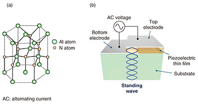
Feature Articles: Forefront Research on Ultrawide-bandgap Semiconductors Vol. 24, No. 6, pp. 41–47, June 2026. https://doi.org/10.53829/ntr202606fa5 Gigahertz Acoustic Wave Devices Using AlN Piezoelectric Thin FilmsAbstractAluminum nitride (AlN), an ultrawide-bandgap semiconductor, exhibits excellent electrical insulation properties as well as high piezoelectricity. Its low mass density compared with other piezoelectric materials makes it a promising candidate for piezoelectric transducers capable of electrically exciting and detecting high-frequency acoustic waves in the gigahertz range. This article introduces NTT’s research on the development of gigahertz acoustic wave devices using high-quality AlN piezoelectric transducers and on the exploration of novel physical phenomena enabled by high-speed acoustic waves. Keywords: aluminum nitride, piezoelectricity, acoustic waves  1. IntroductionAluminum nitride (AlN) has a hexagonal crystal structure known as the wurtzite structure (Fig. 1(a)). A key feature of this structure is the asymmetry of atomic arrangement along the vertical direction within the crystal, resulting in a built-in polarity. When an external force is applied to the crystal and deformation occurs, the relative positions of the Al and nitrogen (N) atoms change, leading to a redistribution of internal charges and the generation of an electric potential. This phenomenon is known as the piezoelectric effect. Conversely, when an electric voltage is applied to the crystal, the atomic positions are displaced along the polar axis, causing the crystal to expand or contract. This is referred to as the inverse piezoelectric effect. Thus, the intrinsic crystal polarity originating from the wurtzite structure makes AlN an excellent piezoelectric material. Because the constituent atoms of the crystal are lightweight, acoustic waves propagate through AlN at high velocities. The propagation velocities are approximately 6,300 m/s for surface acoustic waves (SAWs) and exceed 10,000 m/s for bulk acoustic waves. AlN is thus well suited as a piezoelectric material for high-frequency devices operating in the gigahertz range.
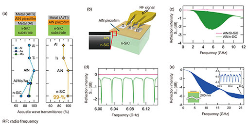
2. Ultrahigh-speed bulk acoustic wave devices using AlN thin filmsWhen an alternating electric field is applied in the vertical direction to the AlN crystal shown in Fig. 1(a), the crystal expands and contracts along the same direction. By exploiting this property, acoustic waves propagating in the thickness direction can be electrically excited by forming a structure in which an AlN thin film is sandwiched between top and bottom electrodes on a substrate. In the structure shown in Fig. 1(b), for example, acoustic waves excited in the piezoelectric thin film propagate into the substrate. When the bulk acoustic waves reach the bottom surface of the substrate, they are reflected and propagate back toward the top surface. As this reflection process repeats, a standing wave is formed when the condition that a node of the wave (a position where the amplitude becomes zero) coincides with the reflecting surface is satisfied, resulting in a stable signal. The formation of this standing wave can be detected through reflection measurements via the electrodes, and a significant reduction in the reflection intensity is observed when the standing wave is excited. Devices that can electrically excite and detect bulk acoustic waves in this manner are referred to as high-overtone bulk acoustic resonators (HBARs)*1 and have recently attracted considerable attention as devices capable of handling high-speed acoustic waves in the gigahertz-frequency range. However, in conventional HBAR structures such as that shown in Fig. 1(b), a metallic electrode layer is interposed between the piezoelectric thin film and substrate. This metal layer causes reflection and attenuation of acoustic waves, resulting in propagation losses into the substrate. To overcome this issue, our research team proposed and demonstrated a novel HBAR that does not require a bottom metal electrode. The key to this device lies in the careful selection of the substrate material. The structure of our HBAR includes a conductive substrate that is lattice-matched to AlN, and an AlN thin film is directly grown on the substrate. The substrate functions as a floating bottom electrode, while lattice matching suppresses acoustic wave propagation losses (Fig. 2(a)). Specifically, N-doped n-type 6H-silicon carbide (SiC)*2 was used as the substrate, and a high-quality AlN thin film was epitaxially grown on it using metal–organic chemical vapor deposition. Our HBAR thus achieved excellent impedance-matching characteristics, enabling ultrahigh-speed acoustic waves to propagate efficiently into the substrate (Fig. 2(b)) [1]. As described above, in an HBAR, elastic waves are repeatedly reflected in the thickness direction, and standing waves are formed under the condition mλ = 2L, where m is an integer, λ is the wavelength of the elastic wave, and L is the total thickness of the device. In our HBAR in which an 800-nm-thick AlN piezoelectric thin film is directly formed on a 0.24-mm-thick n-SiC substrate, for example, a broad resonance spectrum centered around 6 GHz is observed (Fig. 2(c)) together with numerous sharp HBAR modes appearing at regular frequency intervals within this spectrum (Fig. 2(d)) [1]. The resonance frequency of each HBAR mode is given by fm ~ m × vs/2ts, where vs is the acoustic velocity in SiC and ts is the thickness of the SiC substrate. High-quality resonances with quality factors exceeding 103 are obtained. By evaluating the fluctuations in the spacing between adjacent HBAR modes, our HBAR exhibits extremely small impedance mismatch. The center frequency of the broad spectrum shown in Fig. 2(c) is determined by the resonance condition of acoustic waves in the AlN film of thickness tp and is given by fn ~ n × vp/2tp, where n is an integer and vp is the acoustic velocity in AlN*3. Therefore, further thinning of the AlN film is effective for achieving operation at higher frequencies. HBARs with highly optimized impedance matching, as described above, are expected to be used as high-performance oscillators and high-frequency signal filters that surpass conventional devices. Developing ultrahigh-speed HBARs capable of operating in the extremely high-frequency regime approaching 100 GHz is an important future research challenge. Wireless communication technologies such as 5G (fifth-generation mobile communication systems) have advanced rapidly, and the advent of a high-speed communication era using millimeter-wave frequency bands (30–300 GHz), often referred to as Beyond 5G, is imminent. Achieving this will require the development of high-quality acoustic wave devices capable of operating in the millimeter-wave band. Toward this goal, we are pursuing higher-frequency operation through further thinning of AlN piezoelectric films. Figure 2(e) shows the reflection spectrum for our HBAR with an AlN film thickness of 200 nm. In this case, a first-order broad spectrum appears around 10 GHz, and a higher-order broad spectrum is observed around 25 GHz (the higher-order spectrum is also composed of numerous sharp HBAR modes). By thinning the AlN film and using higher-order resonance spectra, HBARs applicable to the millimeter-wave frequency range are anticipated.
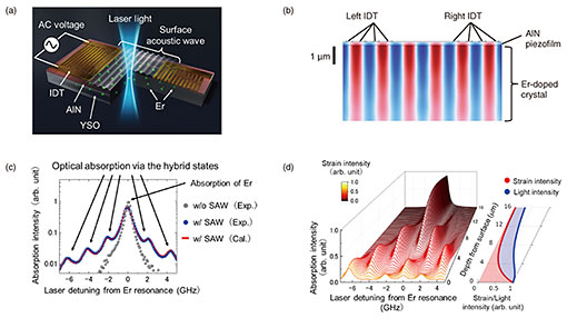
3. Creation of hybrid electron–phonon states using AlN SAW devicesWhile the excitation of ultrahigh-speed acoustic waves exceeding 10 GHz requires the bulk acoustic wave devices described above, acoustic waves below 10 GHz can be electrically excited and detected using SAW devices, which are discussed in the following section. For example, when interdigital transducers (IDTs) are fabricated on an AlN thin film formed on a crystalline substrate and an alternating voltage is applied between the electrodes, SAWs propagating laterally near the surface are excited (Fig. 3(a)). The frequency of the SAWs is determined by the electrode period and acoustic velocity in AlN. For instance, by using IDTs with a period of 0.8 μm, SAWs with a frequency of 2.1 GHz can be excited. The strain associated with the excited SAWs penetrates from the AlN thin film into the underlying substrate; however, its amplitude decays exponentially with depth (Fig. 3(b)). By using such SAW devices, it becomes possible to apply strain to functional materials embedded within the substrate. As an example, we consider a structure in which a 200-nm-thick AlN thin film is sputter-deposited on a rare-earth oxide crystal (yttrium orthosilicate: Y2SiO5) substrate doped with the rare-earth element erbium (Er), which has an excited-electron lifetime on the order of several milliseconds*4 (Fig. 3(a)). In this structure, high-speed strain induced by a 2.1-GHz SAW can be applied to the Er electrons (Fig. 3(b)) [2]. Because the oscillation rate of this strain is much faster than the electronic lifetime of Er, the electronic states are strongly affected by the vibrational strain, leading to the formation of hybrid states resulting from the interaction between electrons and phonons (i.e., acoustic waves). To experimentally observe such unprecedented hybrid states, laser light with a wavelength corresponding to the resonance frequency of the Er electrons (approximately 1.54 μm) was irradiated onto the central region of the SAW device (Fig. 3(a)), and optical absorption spectra were measured via Er photoluminescence. In the optical absorption spectra measured under electrical excitation of SAWs, multiple side peaks appeared in addition to the intrinsic absorption line of Er, with spacings corresponding to the SAW frequency (Fig. 3(c)). These side peaks correspond to absorption by hybridized states of Er electronic states and phonons. By conducting an analysis that takes into account the depth-dependent strain distribution, it is possible to estimate the degree of hybridization as a function of depth within the substrate. The results reveal that no side peaks appear in regions deeper than approximately 12 μm from the crystal surface, whereas near the crystal surface—where the strain effect is strongest—a high degree of hybridization is observed, accompanied by the emergence of several side peaks (Fig. 3(d)). These findings also indicate that, by optically exciting Er ions located near the crystal surface via the side peaks, it may be possible to manipulate the population and phase of excited electrons using acoustic waves [2].
Erbium differs from other rare-earth elements in that it possesses inner-shell electrons resonant with the C-band, a representative wavelength band used in optical communications*4. Because these inner-shell electrons are shielded by outer-shell electrons, they are insensitive to environmental perturbations and can exhibit high quantum coherence, making Er a promising candidate for applications in quantum optical memories. However, this shielding effect also leads to a trade-off in which external controllability of the inner-shell electrons is reduced. In practice, high voltages are required to modulate the resonance frequency of Er using external electric fields, which has been a major challenge. In contrast, the modulation technique for Er electrons using SAWs demonstrated in this study offers high controllability and is expected to pave the way toward novel optical quantum memory devices in which information is written and read out using acoustic waves.
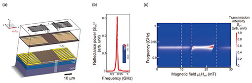
4. Strongly coupled magnon–phonon states using AlN SAW devicesThe SAW technology described above can be extended to a wide variety of material systems beyond luminescent materials. By using structures that incorporate magnetic materials, for example, spin waves (i.e., magnons) and acoustic waves (i.e., phonons) can be strongly coupled via strain induced by SAWs. In particular, single-crystalline yttrium iron garnet (YIG) thin films formed on gadolinium gallium garnet (GGG) substrates are known to support long-lived magnons. By depositing an AlN piezoelectric film on a YIG/GGG substrate and fabricating IDTs on top of the AlN film, it becomes possible to apply the vibrational strain of surface acoustic waves—penetrating beneath the AlN layer—to magnons in the YIG layer. We fabricated a structure consisting of a 5.7-μm-thick single-crystalline YIG film grown on a GGG substrate, 400-nm-thick sputtered AlN piezoelectric film, and gold IDTs with a period of 2 μm formed on top (Fig. 4(a)) [3]. In this structure, SAWs with a frequency of 0.93 GHz can be excited (Fig. 4(b)). When an in-plane magnetic field is applied perpendicular to the IDTs in this device, the magnon resonance frequency can be continuously tuned as a function of the magnetic-field strength. When the magnon resonance frequency coincides with the SAW frequency, strong coupling between magnons and phonons occurs, resulting in a pronounced dip, i.e., mode splitting, in the transmission spectrum of the SAWs. At a magnetic field of 24 mT, for example, the transmission intensity of the acoustic wave is nearly zero, indicating the formation of a fully hybridized magnon–phonon state (Fig. 4(c)). Similar phenomena are also observed around magnetic fields of approximately 14 and 10 mT, which correspond to strong coupling between phonons and first- and second-order magnon modes that possess nodes along the thickness direction of the YIG film [3].
Such strongly coupled magnon–phonon states are expected to enable a wide range of applications, including spin-wave control by acoustic waves (acoustically driven spintronics), acoustic-wave control by spin waves (magnetically driven phononics), and long-distance spin-wave transport mediated by acoustic waves. The information retention capability inherent to magnetic materials opens the possibility of creating novel magnon–phononic devices that go beyond conventional approaches. If similar strong coupling can be achieved using the bulk acoustic wave structures introduced in the first part of this article, ultrahigh-speed magnon–phononic devices operating in the millimeter-wave frequency range would also become feasible. 5. ConclusionWe have introduced gigahertz acoustic wave devices that exploit the excellent piezoelectric properties of AIN. Gigahertz acoustic wave technologies based on AlN piezoelectric thin films extend beyond ultrahigh-speed, high-quality bulk acoustic resonators to the exploration of diverse physical phenomena, including hybrid states of electrons and phonons as well as strong coupling between magnons and phonons. These achievements hold significant potential as enabling technologies for next-generation applications such as high-speed communications, quantum information processing, and energy-efficient signal processing. References
|
|||||||||||||||