|
|||||||||
|
|
|||||||||
|
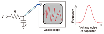
Feature Articles: Frontier Research on Low-dimensional Semiconductor Physics Vol. 13, No. 8, pp. 11–15, Aug. 2015. https://doi.org/10.53829/ntr201508fa3 Noise in Nanometer-scale Electronic DevicesAbstractDownsizing electronic devices in integrated circuits increases the noise-related degradation of circuit performance, and thus, it is becoming more important to analyze noise with single-electron resolution. We discuss here the use of a nanometer-scale transistor and capacitor in analyzing thermal noise, one of the most fundamental types of noise in electronic devices, with single-electron resolution. When the capacitor size is substantially reduced, the well-known model of thermal noise is no longer valid, and voltage noise is squeezed. Keywords: noise, transistor, single electron  1. IntroductionIntegrated circuits comprising silicon transistors and other electronic devices are extremely important components in our information technology society. The transistor, one of the most well-known electrical devices, controls the flow of electricity, that is, electrons, for data processing in the integrated circuits. The performance of such integrated circuits has advanced with the downsizing of transistors; for example, the 14-nm generation of transistors will be reached in 2015. However, downsizing also increases the noise-related degradation of circuit performance, and therefore, a microscopic analysis of noise and the development of countermeasures to such noise have become more important than ever before. Indeed, random telegraph noise originating from single-electron trapping in a transistor becomes prominent in small transistors and gives rise to errors in memory circuits. Shot noise originating from the discrete nature of an electron is also expected to become a serious issue in high-speed integrated circuits. Therefore, the downscaling of the transistors increases not only their performance but also the importance of understanding noise microscopically, ultimately with single-electron resolution, in small transistors as well as in other electronic devices. In this article, we discuss the analysis of thermal noise, one of the most fundamental types of noise in electronic devices, with single-electron resolution using dynamic random access memory (DRAM) composed of a nanometer-scale transistor and capacitor [1]. Because the analysis was done by using a DRAM, one of the most common devices, we believe that our results are relevant to all electronic devices. 2. Techniques for analyzing thermal noiseOne of the simplest and most well-known techniques for analyzing thermal noise is to measure voltage noise in a circuit composed of one resistor and one capacitor, as shown in Fig. 1. In this circuit, a massive number of electrons enter and exit the capacitor through the resistor in a random manner with the assistance of thermal energy. This random motion of electrons is thermal noise, and it exists absolutely at a finite temperature. When voltage noise at a node between the resistor and capacitor is measured with an oscilloscope or voltage meter, we can obtain certain information. For example, we can get a histogram of voltage-noise amplitude based on a Gaussian distribution, whose average is voltage V applied to the resistor. We can also get the variance Vvar2 of the distribution given by kBT/C, where kB is the Boltzmann’s constant, T is temperature, and C is the capacitance of the capacitor. The fact that Vvar2 is proportional to T means that the random motion of electrons originates from thermal energy. In contrast, Vvar2 increases as C decreases, regardless of the resistor. Therefore, the downsizing of electronic devices in circuits such as memory and analog circuits reduces C and thus increases noise, which leads to an undesirable hindrance of device downsizing. These features can be explained by the well-known Johnson-Nyquist model proposed in 1928 [2, 3].
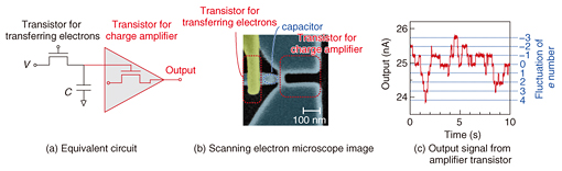
In our technique for analyzing thermal noise with single-electron resolution, we use instead of a resistor a nanometer-scale transistor for transferring the electrons to the capacitor, as shown in Fig. 2(a), because electrical control of the resistance of the transistor helps us to monitor the motion of individual electrons precisely in real time. In a common circuit, time intervals for the electrons to enter and exit the capacitor are too short for the electrons to be monitored: current I of 1 mA corresponds to the time interval of 1.6 × 10⁻¹⁶ (=e/I) seconds, which cannot be measured by any measurement system. However, increasing the resistance of the transistor when it transfers electrons prolongs the interval so that the electron motion can be monitored in real time. These mechanisms and the structure are the same as in a DRAM. Since the charge of an electron is too small (1.6 × 10⁻¹⁹ C) to be detected by any charge sensor, the tiny signal is amplified by using another transistor [4]: The transistor for the charge amplifier has an extremely small channel (~10 nm) and is integrated with the capacitor, as shown in Fig. 2(b). Consequently, the electrons in the capacitor can be detected precisely with single-electron resolution even at room temperature. This success is supported by well-established fabrication techniques for silicon transistors. Using these features, we can monitor the random motion of individual electrons entering and exiting the capacitor through the transistor in real time, as shown in Fig. 2(c): An output signal from the charge-amplifier transistor changes among discrete values, and one gap between these discrete values corresponds to the charge from one electron. To slow down the electron motion so that it can be monitored, the resistance of the transistor used for the electron transfer is adjusted to be around 1020 Ω. This extremely high resistance, which cannot be achieved in conventional resistors and transistors, is possible thanks to our high-quality nanometer-scale transistor.
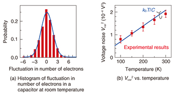
3. Thermal noise with single-electron resolutionIn analyzing the thermal noise with single-electron resolution, we first discuss the fluctuation, that is, the deviation from the average, of the number of electrons in the capacitor. Because single-electron injection into the capacitor increases the voltage of the capacitor by e/C (= dV), the fluctuation of the number of electrons in the capacitor can be converted into a voltage fluctuation, that is, voltage noise, at the capacitor. The dV can be evaluated from the change in the output signal originating from one electron, as shown in Fig. 2(c) [4]. A histogram of the number of electrons in the capacitor is shown in Fig. 3(a). The histogram follows a Gaussian distribution (solid line), as in the case shown in Fig. 1. This histogram gives another piece of information: dV2 multiplied by the variance of the distribution shown in Fig. 3(a) corresponds to Vvar2, and this Vvar2 follows kBT/C, as shown in Fig. 3(b), which is the same as the case where thermal noise originates from the fluctuation of a massive number of electrons, as explained above and as shown in Fig. 1. Consequently, we can conclude that the well-known Johnson-Nyquist model for thermal noise is adaptable to the random motion of single electrons.
However, when charging energy EC (= e2/2C) for injecting one electron into the capacitor is larger than thermal energy kBT, the Johnson-Nyquist model is no longer valid. A histogram of the number of electrons in the capacitor at EC > kBT is shown in Fig. 4(a). Since the distribution (solid line) becomes sharper, and the available number of electrons becomes smaller than in the case of EC < kBT (Fig. 3(a)), the discrepancy between the experimental results (bars) and expected values (solid line) becomes larger in the form of quantization errors in digital circuits. Indeed, Vvar2 (1.08 × 10⁻⁴ V2) evaluated from the variance of the experimental distribution shown in Fig. 4(a) is smaller than kBT/C (1.38 × 10⁻⁴ V2). This deviation from the Johnson-Nyquist model is similar to the case of electromagnetic radiation from a black body. Energy of the electromagnetic radiation is quantized by multiples of hν, where h is Planck’s constant and ν is the frequency of the electromagnetic radiation. Therefore, when a higher ν makes hν larger than thermal energy kBT, the thermal energy cannot assist the emission of electromagnetic waves from the black body. This idea, based on energy quantization proposed by Max Planck, overcomes the ultraviolet catastrophe in the low-frequency region of the spectrum of black-body radiation. Our results for electrons can also be explained qualitatively by the same model as that for the black-body radiation. Energy for injecting N electrons into the capacitor is given by (Ne)2/2C = N2EC and quantized because e is a unit charge. Therefore, as in the case of black-body radiation, when EC is comparable or larger than kBT, the thermal energy cannot assist electrons in entering and exiting the capacitor, which suppresses electron random motion and thus makes Vvar2 smaller than the thermal energy. However, we can observe a unique feature in electron motion unlike in the case of black-body radiation. The average of the number of electrons in the capacitor is given by CV/e, where V is the voltage applied to the transistor as shown in Fig. 2(a). However, for example, when the average number is 0.5, the number of electrons in the capacitor switches between 0 and 1 with the same probability because an electron cannot be divided in half. As a result, the variance of the electron number becomes larger than 0.25, regardless of EC and kBT. In this sense, the fluctuation in the number of electrons depends on the average number of electrons. When the average number is an integer, the fluctuation becomes minimum; when a fractional part of the average number is 0.5, the fluctuation becomes maximum. The change in voltage noise Vvar2 at the capacitor as a function of C is shown in Fig. 4(b). When EC < kBT at larger C, Vvar2 follows kBT/C (open circles) and increases as C decreases. When EC > kBT at smaller C, Vvar2 deviates from kBT/C, and the reduction in C increases the discrepancy between Vvar2 and kBT/C, as indicated by the shaded area depicting the possible values of Vvar2. It should be noted that the minimum border of the shaded area in Fig. 4(b) decreases with C, behavior that is opposite to that of the conventional kBTC-limited case depicted by the open circles. In the conventional case valid at EC < kBT, the reduction in C increases noise, which is a serious issue that hinders the downsizing of electronic devices. However, the case where E > kBT at much smaller C is preferable to the reduction in C due to noise reduction, which accelerates the downsizing of electronic devices.
4. ConclusionAs the downsizing of electronic devices accelerates, thermal noise will continue to deviate from its well-known behavior. However, this does not mean that any new phenomena will appear. Instead, it means that all of the results observed for single electrons follow well-established thermodynamics, for example, a Boltzmann distribution, and are thus valid for all electronic devices. Therefore, we believe that our results are important in the downsizing of devices to achieve a reduction in the number of electrons in the device. Indeed, using nanometer-scale transistors, we have developed memory and data information circuits that use one electron as one bit of information. In these circuits, errors caused by thermal noise represent one of the most serious issues. However, a wider view is that the minimum energy consumed for computation by data information circuits is governed by the thermal energy. Therefore, the analysis of thermal noise is very important for realizing low-power-consumption circuits. References
|
|||||||||