Regular Articles
Vol. 20, No. 11, pp. 73–80, Nov. 2022. https://doi.org/10.53829/ntr202211ra1
Extreme-broadband Analog ICs Based on InP HBT Technology
toward Multi-Tbit/s Optical Communications
Munehiko Nagatani, Teruo Jyo, Hitoshi Wakita,
Tsutomu Takeya, and Hiroyuki Takahashi
Abstract
To cope with the rapid growth of communications traffic, transmission capacity per channel (wavelength) in optical core networks is required to reach the multi-Tbit/s level in the next decade. In this article, we review our latest extreme-broadband analog integrated circuits (ICs), e.g., 110-GHz-bandwidth analog multiplexer/analog de-multiplexer ICs and 200-GHz-bandwidth amplifier, mixer, and combiner ICs, based on our in-house indium phosphide (InP) heterojunction bipolar transistor (HBT) technology that can break through the bandwidth bottlenecks in optical transceivers and be key enablers toward future multi-Tbit/s/ch optical communications systems.
Keywords: analog IC, InP HBT, optical communications
1. Introduction: challenges toward multi-Tbit/s/ch optical communications
Communications traffic has been rapidly increasing due to the spread of broadband applications. In addition, the COVID-19 pandemic has dramatically changed our lifestyles, and various activities and services have migrated to remote and virtual platforms. These changes are further accelerating the growth of communications traffic. Communications networks must continue to increase their capacity to cope with such rapid growth in traffic. Optical core networks require huge-capacity and long-haul transmission systems to accommodate client data and link metropolitan areas as the backbone of the communications infrastructure. Digital coherent technology, which combines coherent detection and digital signal processing, was introduced into optical core networks in the 2010s. Thus far, 100-Gbit/s/ch systems based on 32-GBaud polarization-division-multiplexed (PDM) quadrature phase shift keying (QPSK) and 400-Gbit/s/ch systems consisting of 64-GBaud PDM 16-ary quadrature amplitude modulation (16QAM) have been deployed [1, 2].
To sustain ever-increasing traffic, the transmission capacity per channel (per wavelength) is expected to exceed 1 Tbit/s in the near future and reach multi-Tbit/s in the 2030s. Channel capacity is defined as the product of the symbol rate and modulation order, so it can be improved by increasing the symbol rate and/or modulation order, as illustrated in Fig. 1. Increasing the symbol rate while maintaining a low modulation order is advantageous for constructing long-haul transmission systems because higher-order modulation faces optical signal-to-noise-ratio limitation due to amplified spontaneous emission noise and fiber-nonlinearity in the optical links, shortening transmission distance. Therefore, a symbol rate of over 200 GBaud is necessary to construct future multi-Tbit/s/ch long-haul optical transmission systems. This means that each building block in an optical transceiver is required to have an analog bandwidth of at least 100 GHz, which is a Nyquist frequency of 200 GBaud. One of the most significant challenges in constructing multi-Tbit/s/ch systems is implementing extreme-broadband digital-to-analog converters (DACs) and analog-to-digital converters (ADCs) in the optical transceiver. To address this challenge, we previously proposed and intensively investigated bandwidth doubler technology [3, 4] based on analog multiplexer (AMUX) and analog de-multiplexer (ADEMUX) integrated circuits (ICs) that can double the bandwidth of DACs and ADCs, respectively, as illustrated in Fig. 2.
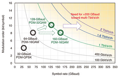
Fig. 1. Channel capacity: symbol rate versus modulation order.
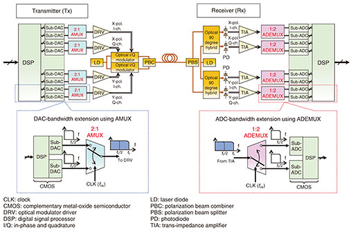
Fig. 2. Our bandwidth doubler technology using 2:1 AMUX and 1:2 ADEMUX.
This article reviews our latest extreme-broadband analog ICs, e.g., 110-GHz-bandwidth AMUX/ADEMUX ICs [5, 6] and 200-GHz-bandwidth amplifier, mixer, and combiner ICs [7–10], based on our in-house 250-nm indium phosphide (InP) heterojunction bipolar transistor (HBT) technology [11] that enable further bandwidth extension.
2. 110-GHz-bandwidth AMUX and ADEMUX ICs
We designed and fabricated AMUX and ADEMUX ICs using our in-house 250-nm InP HBT technology [11]. Figures 3(a) and (b) show a scanning electron microscopy (SEM) image and cross-section of our InP HBT. The HBT layer structure was grown on a 3-in InP substrate and consists of a degenerately doped indium gallium arsenide (InGaAs) emitter contact, 20-nm-thick InP emitter, 25-nm-thick compositionally graded InGaAs base, 100-nm-thick InGaAs/indium aluminum gallium arsenide (InAlGaAs)/InP collector, and InGaAs/InP subcollector. The HBTs have a peak cutoff frequency (fT) and maximum oscillation frequency (fmax) of 460 and 480 GHz, respectively, as show in Fig. 3(c). They also exhibit a common-emitter breakdown voltage (BVCEO) of 3.5 V. Thus, the InP HBTs have both high-speed and high breakdown voltage characteristics and suitable for implementing broadband and high output power circuits.
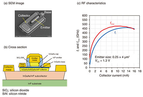
Fig. 3. Our InP HBT: (a) SEM image, (b) cross section, and (c) radio-frequency (RF) characteristics.
The 2:1 AMUX IC is composed of two input linear buffers, a clock limiting buffer, AMUX core based on Gilbert-cell selector circuitry, and output linear buffer, as shown in Fig. 4(a). The detailed transistor-level structures are described in a previous study [5]. All the building blocks in the AMUX IC have fully differential configurations. Figure 4(b) shows a microphotograph of the 2:1 AMUX IC. The chip is 2 mm2 and contains 210 HBTs and consumes a total power of 0.90 W with a single power-supply voltage of –4.5 V. Figure 4(c) shows the measured and simulated S-parameters for the analog signal path in through mode. The measured 3-dB bandwidth was over 110 GHz and agreed well with the simulation. These results indicate that this AMUX IC enables us to generate 200-GBaud-class baseband signals.
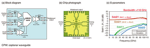
Fig. 4. 2:1 AMUX IC: (a) block diagram, (b) chip photograph, and (c) S-parameters.
A block diagram of the 1:2 ADEMUX IC is shown in Fig. 5(a). This IC consists of input linear buffers, clock limiting buffers, an ADEMUX core based on two parallel track-and-hold (T/H) circuits, and output linear buffers. The T/H circuit in the ADEMUX core is composed of switched emitter followers and hold capacitors [6]. The other blocks have similar topologies with the blocks used in the AMUX IC. Figure 5(b) is a microphotograph of the 1:2 ADEMUX IC. The chip size is also 2 mm2 and has 320 integrated HBTs. The ADEMUX IC dissipates a power consumption of 1.14 W with a –4.5-V power supply. The measured and simulated S-parameters for the analog signal path in track mode are shown in Fig. 5(c). The measured 3-dB bandwidth was 110 GHz and agreed with the simulations, as expected. These results also indicate that this ADEMUX IC can be used to receive 200-GBaud-class baseband signals.
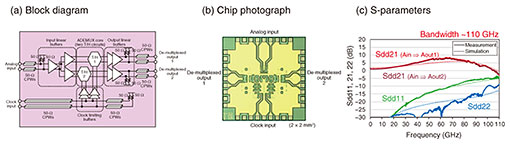
Fig. 5. 1:2 ADEMUX IC: (a) block diagram, (b) chip photograph, and (c) S-parameters.
We have already succeeded in demonstrating various record ultrahigh-speed optical transmission experiments using an AMUX-integrated optical transmitter front-end module [5], such as a 200-GBaud-class optical modulation [12] and beyond-1-Tbit/s/ch over-1000-km long-haul optical transmissions [13]. Thus, the AMUX and ADEMUX ICs can be key enablers for next generation 200-GBaud-class long-haul optical transmission systems.
3. 200-GHz-bandwidth amplifier, mixer, and combiner ICs
Toward future multi-Tbit/s/ch systems with a symbol rate of over 200 GBaud, we proposed and investigated bandwidth-extension techniques [7–10], as illustrated in the conceptual block diagrams (Fig. 6). On the transmitter side, the signal bandwidth can be doubled using a mixer, amplifier, and combiner. On the receiver side, however, the signal bandwidth can also be doubled using an amplifier (splitter) and mixer. We have designed and fabricated amplifier, mixer, and combiner IC prototypes that have a bandwidth of 200 GHz, which is twice that of the AMUX and ADEMUX ICs described in the previous section, using the same InP HBT.
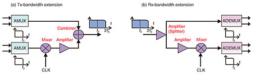
Fig. 6. Bandwidth-extension techniques using amplifier, mixer, and combiner: (a) Tx-bandwidth extension and (b) Rx-bandwidth extension.
Figure 7(a) shows a schematic of the amplifier IC. We applied a distributed circuit topology to the amplifier to achieve a broad gain profile and impedance matching. The distributed amplifier consists of six unit gain cells, coplanar waveguide (CPW) transmission lines, and termination resistors. Multi-peaking techniques were proposed to make broad-peaking characteristics to compensate for loss derived from the packaging and subsequent components [7, 8]. A microphotograph of the fabricated amplifier IC is shown in Fig. 7(b). The IC is 0.95 × 0.87 mm and consumes 0.54 W of power with –4.5-V supply voltage. Figure 7(c) shows the measured S-parameters. The direct current (DC) gain and 3-dB bandwidth were 7.5 dB and 208 GHz, respectively.
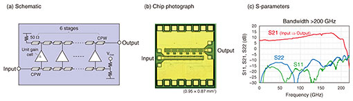
Fig. 7. Amplifier IC: (a) schematic, (b) chip photograph, and (c) S-parameters.
Figure 8(a) is a schematic of the mixer IC. The mixer is based on a distributed topology and composed of six unit cells, each of which is a single-balanced mixer circuitry [9]. One of the differential outputs is terminated inside this prototype for testing. Figure 8(b) shows a microphotograph of the fabricated mixer IC. The chip size is approximately 0.8 mm2. The power consumption is 0.13 W with a supply voltage of –3.8 V. The measured conversion gain (CG) and S-parameters are shown in Fig. 8(c). The clock signal was set to 97.2 GHz for CG measurement. The CG is –3 dB in low frequency range. The output covers the frequency range from DC to approximately 200 GHz. This mixer has the broadest bandwidth of any previously reported mixers.
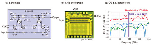
Fig. 8. Mixer IC: (a) schematic, (b) chip photograph, and (c) CG and S-parameters.
A schematic of the combiner IC is illustrated in Fig. 9(a). It consists of two parallel distributed amplifiers and a subsequent distributed resistive combiner [10]. This architecture helps in achieving both broadband characteristics and good isolation between two input ports. Figure 9(b) shows a microphotograph of the combiner IC, which is 0.8 mm2. The power dissipation is 1.1 W from a supply of –4.5 V. The measured S-parameters are shown in Fig. 9(c). The measured 3-dB bandwidth is over 220 GHz, which is the broadest reported to date.
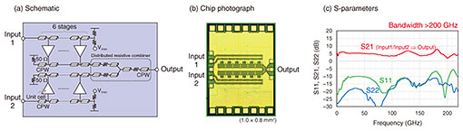
Fig. 9. Combiner IC: (a) schematic, (b) chip photograph, and (c) S-parameters.
We have succeeded in fabricating extreme-broadband amplifier, mixer, and combiner ICs that have a bandwidth of 200 GHz. They enable us to handle 400-GBaud-class signals. Thus, these extreme-broadband ICs could be key to future multi-Tbit/s/ch systems.
4. Summary
We reviewed our latest extreme-broadband analog ICs that can break through the bandwidth bottlenecks in transceivers toward multi-Tbit/s/ch optical communications. We will accelerate investigations for the practical application of these analog ICs and pursue further extreme performance to ensure sustainable progress of communications technologies.
References
| [1] |
Y. Miyamoto, K. Watanabe, and K. Nakajima, “Research and Development of Scalable Optical Transport Technologies,” NTT Technical Review, Vol. 20, No. 7, pp. 24–29, 2022.
https://doi.org/10.53829/ntr202207fa3 |
| [2] |
Y. Kisaka, E. Yamazaki, H. Nishizawa, and T. Saida, “Future Development of Digital Coherent Optical Transmission Technology,” NTT Technical Review, Vol. 20, No. 7, pp. 17–23, 2022.
https://doi.org/10.53829/ntr202207fa2 |
| [3] |
M. Nagatani, H. Wakita, Y. Ogiso, H. Yamazaki, M. Ida, and H. Nosaka, “Ultrahigh-speed Optical Front-end Device Technology for Beyond-100-GBaud Optical Transmission Systems,” NTT Technical Review, Vol. 17, No. 5, pp. 27–33, 2019.
https://www.ntt-review.jp/archive/ntttechnical.php?contents=ntr201905fa4.html |
| [4] |
Press release issued by NTT, “World’s first experimental long-distance WDM optical transmission at 1 Tbps per wavelength—Expected to provide large-capacity network communications for IoT and 5G services,” Mar. 7, 2019.
https://group.ntt/en/newsrelease/2019/03/07/190307a.html |
| [5] |
M. Nagatani, H. Wakita, H. Yamazaki, Y. Ogiso, M. Mutoh, M. Ida, F. Hamaoka, M. Nakamura, T. Kobayashi, Y. Miyamoto, and H. Nosaka, “A Beyond-1-Tb/s Coherent Optical Transmitter Front-end Based on 110-GHz-bandwidth 2:1 Analog Multiplexer in 250-nm InP DHBT,” IEEE J. Solid-State Circuits, Vol. 55, No. 9, pp. 2301–2315, 2020. |
| [6] |
M. Nagatani, H. Wakita, T. Jyo, T. Takeya, H. Yamazaki, Y. Ogiso, M. Mutoh, Y. Shiratori, M. Ida, F. Hamaoka, M. Nakamura, T. Kobayashi, H. Takahashi, and Y. Miyamoto, “110-GHz-bandwidth InP-HBT AMUX/ADEMUX Circuits for Beyond-1-Tb/s/ch Digital Coherent Optical Transceivers,” Proc. of IEEE Custom Integrated Circuits Conference (CICC), Newport Beach, CA, USA, Apr. 2022. |
| [7] |
T. Jyo, M. Nagatani, M. Ida, M. Mutoh, H. Wakita, N. Terao, and H. Nosaka, “A 241-GHz-bandwidth Distributed Amplifier with 10-dBm P1dB in 0.25-µm InP DHBT Technology,” Proc. of IEEE MTT-S International Microwave Symposium (IMS), pp. 1430–1433, Boston, MA, USA, June 2019. |
| [8] |
T. Jyo, M. Nagatani, M. Mutoh, Y. Shiratori, H. Wakita, and H. Takahashi, “An Over 130-GHz-bandwidth InP-DHBT Baseband Amplifier Module,” Proc. of IEEE BiCMOS and Compound Semiconductor Integrated Circuits and Technology Symposium (BCICTS), Monterey, CA, USA, Dec. 2021. |
| [9] |
T. Jyo, M. Nagatani, M. Ida, M. Mutoh, H. Wakita, N. Terao, and H. Nosaka, “A DC to 194-GHz Distributed Mixer in 250-nm InP DHBT Technology,” Proc. of IEEE MTT-S International Microwave Symposium (IMS), pp. 771–774, Virtual, Aug. 2020. |
| [10] |
T. Jyo, M. Nagatani, M. Ida, M. Mutoh, H. Wakita, N. Terao, and H. Nosaka, “An over 220-GHz-bandwidth Distributed Active Power Combiner in 250-nm InP DHBT,” Proc. of BCICTS 2020, Virtual, Nov. 2020. |
| [11] |
N. Kashio, K. Kurishima, M. Ida, and H. Matsuzaki, “Over 450-GHz ft and fmax InP/InGaAs DHBTs with a Passivation Ledge Fabricated by Utilizing SiN/SiO2 Sidewall Spacers,” IEEE Trans. Electron Devices, Vol. 61, No. 10, pp. 3423–3428, 2014. |
| [12] |
M. Nakamura, F. Hamaoka, M. Nagatani, Y. Ogiso, H. Wakita, H. Yamazaki, T. Kobayashi, M. Ida, H. Nosaka, and Y. Miyamoto, “192-Gbuad Signal Generation using Ultra-broadband Optical Frontend Module Integrated with Bandwidth Multiplexing Function,” Proc. of 2019 Optical Fiber Communications Conference (OFC 2019), San Diego, CA, USA, Mar. 2019. |
| [13] |
M. Nakamura, T. Sasai, K. Saito, F. Hamaoka, T. Kobayashi, H. Yamazaki, M. Nagatani, Y. Ogiso, H. Wakita, Y. Kisaka, and Y. Miyamoto, “1.0-Tb/s/λ 3840-km and 1.2-Tb/s/λ 1280-km Transmissions with 168-GBaud PCS-QAM Signals Based on AMUX Integrated Frontend Module,” Proc. of OFC 2022, W3C.1, San Diego, CA, USA, Mar. 2022 |
 |
- Munehiko Nagatani
- Distinguished Researcher, NTT Device Technology Laboratories and NTT Network Innovation Laboratories.
He received an M.S. and Ph.D. in electrical and electronics engineering from Sophia University, Tokyo, in 2007 and 2021. He joined NTT Photonics Laboratories in 2007, where he engaged in the research and development (R&D) of ultrahigh-speed analog and mixed-signal ICs for optical communications systems. He is currently with NTT Device Technology Laboratories and NTT Network Innovation Laboratories, where he is involved in R&D of extreme-broadband ICs for communications and emerging applications. He received the Institute of Electronics, Information and Communication Engineers (IEICE) Young Researcher’s Award in 2011, the 67th Maejima Hisoka Encouragement Award in 2022, and the Commendation for Science and Technology by the Minister of Education, Culture, Sports, Science and Technology, the Young Scientists’ Award in 2022. He served as a technical program committee (TPC) member for Institute of Electrical and Electronics Engineers (IEEE) Compound Semiconductor Integrated Circuits Symposium (CSICS) from 2014 to 2017. He has been serving as a TPC member for IEEE BiCMOS and Compound Semiconductor Integrated Circuits and Technology Symposium (BCICTS) since 2018 and IEEE International Solid-State Circuits Conference (ISSCC) since 2019. He is a member of IEICE and IEEE.
|
 |
- Teruo Jyo
- Researcher, NTT Device Technology Laboratories.
He received a B.E. and M.E. in electronic engineering from Keio University, Kanagawa, in 2012 and 2014. In 2014, he joined NTT Microsystem Integration Laboratories. He is currently a researcher at NTT Device Technology Laboratories. His research interests are high-speed analog circuits for optical fiber communications and terahertz-wave wireless communications and imaging. He received the 2013 IEEE Radio and Wireless Symposium (RWS) Best Student Poster Award and the 2019 IEEE Microwave Theory and Techniques Society (MTT-S) Japan Young Engineer Award.
|
 |
- Hitoshi Wakita
- Researcher, NTT Device Technology Laboratories.
He received a B.S. in organic and polymeric materials in 2008 and M.S. in chemistry and materials science in 2010 from Tokyo Institute of Technology. In 2010, he joined NTT Photonics Laboratories, where he has been engaged in R&D of ultrahigh-speed mixed-signal ICs and modules for optical communications systems. He is currently with NTT Device Technology Laboratories. He is a member of IEICE and IEEE.
|
 |
- Tsutomu Takeya
- Researcher, NTT Device Technology Laboratories.
He received a B.S., M.S., and Ph.D. in electrical engineering from Keio University, Kanagawa, in 2008, 2010, and 2013. He joined NTT Microsystem Integration Laboratories in 2013, where he engaged in the research of analog and mixed-signal ICs for optical communications. From 2016 to 2020, he was with NTT Electronics, where he engaged in the development of digital coherent DSP for optical communication. He is currently with NTT Device Technology Laboratories researching high-speed analog ICs. He is a member of IEICE and IEEE.
|
 |
- Hiroyuki Takahashi
- Senior Research Engineer, Supervisor, NTT Device Technology Laboratories.
He received a B.S. and M.S. in applied physics from Nagoya University in 2001 and 2003. He also received a Ph.D. in advanced electronics and optical science from Osaka University in 2014. In 2003, he joined NTT Microsystem Integration Laboratories. He is engaged in R&D of millimeter-wave/terahertz monolithic microwave ICs. His other research interests include ultrahigh-speed wireless technologies. He was the recipient of the 2008 Young Engineers Prize presented at the European Microwave Integrated Circuits Conference, the 2009 Radio Achievement Award of the Association of Radio Industries and Businesses, the 2010 Asia-Pacific Microwave Conference (APMC) Prize, the 2012 IEEE MTT-S Japan Young Engineer Award, and the 2012 APMC Prize. He is a member of the IEEE MTT-S and IEICE.
|
↑ TOP
|

