|
|||||||||||||||||||||||||||||||||||||||||||||
|
|
|||||||||||||||||||||||||||||||||||||||||||||
       |
Letters Vol. 5, No. 6, pp. 31–36, June 2007. https://doi.org/10.53829/ntr200706le1 Operation of Silicon Single-electron Devices at Room TemperatureAbstractWe report the development of devices for single-electron transfer and detection at room temperature, using silicon metal-oxide-semiconductor field-effect transistors (MOSFETs). Single electrons are transferred one by one to a storage node just by alternately turning two MOSFETs on and off. Electron confinement using an electric field achieves the single-electron transfer at room temperature. Another MOSFET, located close to the storage node, detects electrons transferred into the node with single-electron resolution. These transfer and detection functions were applied to a data processing circuit using a single electron to represent one bit of information. 
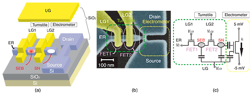
1. IntroductionSingle-electron devices, first advocated in the late 1980s [1], have been studied from the viewpoints of various applications, e.g., digital and analog integrated circuits for ultralow power consumption [2], [3], sensors [4], and metrological tools [5]. The operating principle of the basic single-electron device (SED) is based on the Coulomb blockade, which prohibits single electrons from passing through a tunnel junction into a tiny conductive island [1]. The first SED was made of metal [6]. Since that pioneering work, various materials, such as compound semiconductors [7], Si [8], and carbon nanotubes [9], have been researched. Among these, Si has great advantages: it offers SEDs with highly stable characteristics [10] and fabrication processes that are compatible with those for Si integrated circuits. More fascinating is the possibility that Si-based SEDs with a single-electron transfer function [11]–[14] could offer a promising way to make the ultimate circuits that use one electron to represent one bit of information because of the simple structure and operation of Si SEDs compared with those made of other materials [5]. Room-temperature single-electron transfer, however, has been a tremendous challenge because of the extreme difficulty of making conductive islands small enough (<10 nm) for the Coulomb blockade to overcome the thermal energy. In addition, for implementation in real applications, the small signal originating from single electrons must be detected with high precision to enable us to access the processed/calculated data (i.e., single electrons). In this article, we report the development of a device that can both transfer and detect single electrons at room temperature. The device, fabricated using MOSFET technology, was applied to a single-electron-based digital-to-analog (D/A) converter [15] that can be used in single-electron-based logic applications. 2. FabricationThe device comprises two key elements: a single-electron turnstile to transfer electrons one by one and an electrometer to detect single electrons (Fig. 1(a)). First, a one-dimensional wire for the turnstile and a narrow constriction for the electrometer were patterned on a 30-nm-thick silicon-on-insulator layer. The widths of the one-dimensional wire and constriction were 80 and 35 nm, respectively. This was followed by thermal oxidation. This oxidation process formed 40-nm-thick SiO2 and converted the constriction into a tiny channel, which was used as an electrometer. Then, two gate electrodes made of phosphorous-doped poly-Si were formed on the one-dimensional wire (Fig. 1(b)). The gate lengths and the pitch between the two gates were 50 and 100 nm, respectively. These gates, hereafter referred to as lower gates (LG1 and LG2), constitute two one-dimensional MOSFETs (FET1 and FET2) for the turnstile. The tip part of FET2, which was capacitively coupled to the channel of the electrometer, acted as a storage node (SN). A small single-electron box (SEB) was formed in the channel between FET1 and FET2. The subsequent oxidation reduced the gate length to 20 nm. Finally, a 50-nm-thick oxide layer and an upper gate (UG) were formed. The UG, which covered the entire region shown in Fig. 1(b), was used to make electrons accumulate in the Si layer and to control the potential of the SN and SEB. The equivalent circuit of the fabricated device is shown in Fig. 1(c). Electrons were transferred between an electron reservoir (ER) and the SN through FET1 and FET2. The electrons that had been transferred to the SN were then detected using the electrometer.
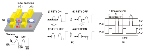
3. Principle3.1 Single-electron turnstileFigure 2 explains how electrons are transferred one by one to the SN by means of the single-electron turnstile. The initial condition is that the OFF-state FET1 and FET2 raise potential barriers under LG1 and LG2, respectively, in the wire channel and thus form the SEB and SN, as shown in Fig. 2(a). When FET1 turns ON (step (i) in Fig. 2(a)), electrons enter the SEB via FET1 from the ER. As FET1 turns from ON to OFF, the potential barrier under LG1 rises and the SEB is electrically isolated from the ER (step (ii)). Since the SEB is small enough for the Coulomb blockade to be prominent, some electrons flow out of the SEB and return to the ER via FET1, and a single electron remains in the SEB. Next, FET2 turns from OFF to ON, and the electron in the SEB is transferred to the SN because the energy potential in the SEB is higher than that in the SN (step (iii)). In step (iv), FET2 completely closes and the electron remains in the SN. These four steps comprise one cycle for injecting a single electron into the SN. Although electrons are accumulated in the SN in each cycle, the single-electron transfer happens correctly by the same mechanism until the repulsive force between electrons becomes prominent.
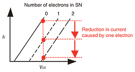
Most importantly, the SEB should be small enough for single-electron transfer at room temperature. Since its size is basically defined by the gap between LG1 and LG2, we narrowed the gap to 80 nm by using a fine patterning lithography process. However, this lithographically defined SEB size was still not small enough for room-temperature operation. Thus, we applied an electric field to the fabricated device to further shrink the SEB: depletion regions extending from the two gates, which turn the MOSFETs off, confined electrons midway between FET1 and FET2, and the Si substrate was negatively biased so that electrons were confined near the top of the channel [16]. As a result, the operating temperature could be increased to 300 K. 3.2 Single-electron detectionThe single electrons transferred to the SN are subsequently detected by the electrometer; the current IE flowing through the electrometer at constant VUG is changed because the electrometer's current characteristics are shifted by transferred electrons, due to the capacitive coupling between the SN and electrometer, as shown in Fig. 3 [17]. Since a charge sensitivity high enough to detect single electrons requires a large change in IE , i.e., large capacitive coupling between the SN and electrometer, we narrowed the gap between the SN and electrometer to 80 nm by using fine patterning lithography and reduced the size of the electrometer channel to less than 10 nm by oxidation. As a result, the charge sensitivity reached 0.005e/√Hz at 2 Hz, even at room temperature.
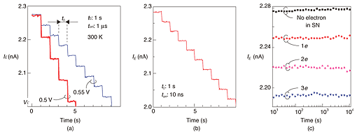
4. Experimental results at room temperature4.1 Single-electron transfer and detectionChanges in the electrometer current when the transfer cycles shown in Fig. 2(b) were repeated are shown in Fig. 4(a). Abrupt changes appeared when FET2 turned on. In the blue line, the height of each step corresponds to the shift in IE characteristics, as shown in Fig. 3. Changing the ER voltage VE made the height of each step in the red line twice that in the blue one. These features indicate that the discrete changes in current represented by the blue and red lines resulted from single- and double-electron transfer, respectively, in one transfer cycle [15]. Moreover, an analysis of the success rate of single-electron transfer proves that the Coulomb blockade was effective for the accurate transfer of single electrons, which caused the discrete change in electrometer current [15]. These results mean that the device fabricated with MOSFET technology achieved the functions of both single-electron transfer and subsequent detection.
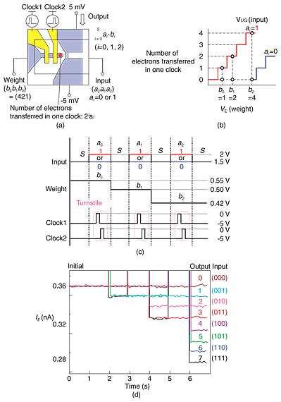
The MOSFET-based turnstile has the unique features of both fast electron transfer (10 ns) and a long retention time (104 s), as shown in Figs. 4(b) and (c), respectively. This is because the ON- and OFF-state MOSFETs make its channel resistance lower for electron transport and higher for retention, respectively. It should be pointed out that the MOSFET-based turnstile overcomes the tradeoff between electron transfer speed and retention time that is inevitable in SEDs that have tunnel barriers with constant resistance [18]. 4.2 D/A converter using single electronsOne novel application of single-electron-based circuits is the time-division weighted sum operation. Its operating principle is shown in Fig. 5(a). Assume that 3-bit binary input signals (a2a1a0) and weight signals (b2b1b0) are applied to the UG and ER, respectively. The key point is that the number of electrons transferred in one transfer cycle (clock) as a function of VE (weight) can be controlled by VUG (input), as shown in Fig. 5(b). When ai (i=0, 1, 2) is 1, the number of electrons transferred in one clock is controlled by the weight signal bi applied to the ER, which allows the number of electrons transferred in one clock to be 2i for the D/A converter operation. When ai is 0, no electrons are transferred regardless of bi. Thus, when we apply ai and bi sequentially together with a clock in parallel at each i, as shown in Fig. 5(c), the total number of electrons in the SN is
When bi is adjusted so that the number of electrons transferred in one clock is 2i, this circuit acts as a D/A converter, in which a binary signal is converted into the number of electrons in the SN. The periods in the input signals during which the number of electrons in the SN is measured after each ai has been input are referred to as standby periods S. During a standby period, VUG (input) is the same as when ai is 0. In fact, since standby periods are useful only for monitoring the operation step by step for clear experiments and are not essential to the operation, they can be removed. Some experimental results are shown in Fig. 5(d). Since the electrometer current IE was over 2 nA when ai = 1, we focused on the electrometer current IE during standby periods for clarity. Just after each period of ai = 1, IE was changed from the value in the previous standby period. This means that the number of electrons transferred while ai = 1 was 2iai. Finally, binary 3-bit signals were converted into a signal with a magnitude of which was expressed by an 8-level electrometer current. This process corresponds to the function of D/A conversion. This time-division conversion could be done using only one device because electrons were transferred and stored one after another in the SN regardless of the presence of previously transferred electrons. This demonstration shows that the fabricated device offers a way to make a fundamental component that will serve as a bridge between conventional binary signals and those used in various single-electron-based circuits.
5. ConclusionWe have fabricated a device with a single-electron turnstile and electrometer using MOSFET technology that should be commercially available by 2009. Electron confinement using gates can make the single-electron box of the turnstile small enough for single electrons to be transferred at room temperature. Moreover, the dynamically controllable barrier provides fast electron transfer as well as long retention. As an application using these features, a time-division weighted sum circuit has been demonstrated at room temperature. The great similarity between the fabricated devices and conventional MOSFETs should allow the large-scale integration of single-electron devices. References
|
||||||||||||||||||||||||||||||||||||||||||||