|
|||||||||||||||||||||||||||||
|
|
|||||||||||||||||||||||||||||
       |
Selected Papers: MEMS Device Technologies Vol. 5, No. 10, pp. 6–10, Oct. 2007. https://doi.org/10.53829/ntr200710sp1 MEMS Device Technology for Ubiquitous ServicesAbstractThis paper introduces microelectromechanical systems (MEMS) device technology at NTT Laboratories as a key hardware technology for achieving ubiquitous services based on novel functions in various fields such as information communications, security, and biotechnology. 
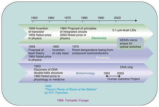
1. IntroductionMEMS stands for microelectromechanical systems. It is an enabling technology that uses semiconductor microfabrication processes to develop integrated devices containing movable mechanical elements and electrical elements from the submicrometer level up to sizes of about one millimeter. MEMS promises to provide key high-performance devices featuring energy-saving characteristics, compact configurations, and high accuracy applicable to a diverse range of fields such as information communications, security, and biotechnology. No doubt many readers have heard of the 1966 science fiction film “Fantastic Voyage”. To save an important person suffering from a blood clot in the brain, a submarine with a crew including doctors and scientists is shrunk to microscopic size and injected into the person's bloodstream in an effort to destroy the clot. At the time of the film's release, this was a completely fantastic idea, as the name of the movie implies. Of course, sending people into a person's body is just a fantasy, but the idea of treating the body from the inside is starting to take shape through devices such as ingestible endoscopy capsules. The microdevice concept dates back nearly 50 years to a famous lecture entitled “There's Plenty of Room at the Bottom” given by Richard Feynman, who later was a joint recipient of the Nobel prize, at a 1959 meeting of the American Physical Society held at the California Institute of Technology [1]. In that lecture, Feynman mentioned the possibility of micromachines consisting of several thousand atoms. The lecture title means that there are still unexplored regions at the submicroscopic scale that mankind should investigate through science and technology. A chronology of inventions and discoveries that have become a basis for MEMS-related technologies is given in Fig. 1. Also given are the years of Nobel prizes awarded in recognition of these ground-breaking efforts. We can see that a number of great inventions and discoveries in the microworld that have become the basis for information communications and biotechnology of the present were made in the ten-year periods before and after Feynman's lecture. These include the invention of the transistor, proposal of basic principles underlying integrated circuits, discovery of the double-helix structure of DNA, and invention of the laser.
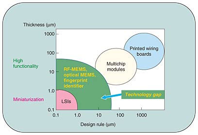
We can view MEMS as technology for integrating in the microworld these inventions and discoveries of 20th-century science and technology for use in information communications, biotechnology, and other fields, and as a means for fabricating 21st-century devices and systems. At present, MEMS-related development proceeds on a field-by-field basis, such as optical-MEMS for optical communications, RF-MEMS for wireless communications including cell phones (RF: radio frequency), and bio-MEMS for medical care and biotechnology. 2. MEMS and technology gapNTT Microsystem Integration Laboratories has the mission of creating key hardware-oriented technologies to achieve a network environment that can provide safe, secure, and enjoyable broadband and ubiquitous services, as promoted by the NTT Group. At these laboratories, MEMS is positioned as a platform technology for creating ubiquitous services. The graph in Fig. 2 shows device design rule on the horizontal axis and film thickness on the vertical axis. RF-MEMS and optical-MEMS devices lie in the intermediate region between miniature devices like LSIs (large-scale integrated circuits) and Jisso technologies*1 like multichip modules and printed wired boards. Jisso technologies have an important role in enabling MEMS devices with microscopic movable mechanical elements to interface with the outside world. Existing technologies used for Jisso, however, target elements with sizes of several micrometers to several millimeters or more, and they cannot by themselves be used to fabricate tiny MEMS devices.
If, however, submicrometer LSIs and MEMS devices using LSI fabrication technology can be fabricated and integrated on a silicon substrate, we can expect even greater downsizing and greater functionality including enhanced intelligence in MEMS devices. Yet, technology for fabricating LSIs is specialized for ultramicrofabrication, and it too is not necessarily applicable to the fabrication of MEMS devices. This leaves MEMS devices lying in a technology gap between LSIs and Jisso technologies. Consequently, despite the great expectations that MEMS has been generating, only a few MEMS devices have been successful in business, such as inkjet printer heads.
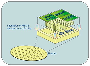
3. Seamless integration technologyTo fill in this technology gap, NTT Microsystem Integration Laboratories is developing technology that uses the silicon technology cultivated with LSIs as a core technology for fabricating and converging ultrafine LSIs and MEMS devices on a silicon wafer while providing a seamless bridge to Jisso technologies. This seamless integration technology (SeaiT), as it is known, aims to achieve smooth convergence between the heterogeneous functions performed by microelectronics and micromachines [2], [3]. As shown in Fig. 3, seamless integration technology for converging LSI and MEMS is intended to fabricate microscopic MEMS devices and wiring with a size of 10 µm to 1 mm made of metal or silicon in a layered manner. This calls for fabrication technology that will produce little damage to the LSI. Specifically, it must be a low-temperature process and must not use dry etching, which could damage LSIs, for example. Accordingly, to form MEMS structures without incurring such damage, we are developing low-temperature plating techniques as well as 10-µm-level thick-film multilevel interconnection technology using photosensitive organic resins and other advanced materials [4].
4. Toward high-yield and high-reliability MEMS devicesMEMS devices feature microscopic movable mechanical elements. A typical example is the switches in RF-MEMS devices. To prevent damage to movable parts and achieve high-yield fabrication of these devices, we need a technology that can protect movable parts until their packaging is completed. To this end, we are developing a spin-coating film transfer and hot-pressing (STP) technology [5], i.e., a film-growth technology for sealing movable parts, to be used from the materials/process stage to the device stage. Microscopic movable mechanical elements can also become affixed to an electrode and stop moving in the course of being driven an excessive voltage. This “sticking” phenomenon is a particular problem for MEMS devices having movable parts. Once sticking occurs, the movability cannot be restored, so it is important that this problem is addressed if MEMS devices having movable mechanical elements are to become practical. Studies are now being performed on a technique for preventing sticking and achieving high-reliability driving of MEMS devices by coating movable parts and electrodes with electrodeposited organic thin films [6]. 5. MEMS devices in developmentSeamless integration technology enables the formation on LSIs with structures having dimensions or thicknesses that are hard to achieve by existing technologies. This should lead to highly functional MEMS chips featuring an array of MEMS devices or MEMS that integrate new functions that could not be achieved with LSIs or existing MEMS devices alone. With the aim of providing safe and secure ubiquitous services, NTT Microsystem Integration Laboratories is developing a MEMS fingerprint authentication sensor [7], a MEMS mirror array as an element of a MEMS optical switch module [8] (a key device in the next-generation network), and an RF-MEMS chip for wireless terminals [9]. The other selected papers in this issue describe seamless integration technology in more detail and introduce these MEMS devices. 6. ConclusionLooking to the future, we plan to develop various MEMS devices and increase their level of integration and functionality with the aim of refining our seamless integration technology and achieving safe, secure, and enjoyable ubiquitous services. References
|
||||||||||||||||||||||||||||