|
|||||||||||||||||||||||||||
|
|
|||||||||||||||||||||||||||
       |
Special Feature: EMC Technology for IP Network Infrastructure Vol. 5, No. 12, pp. 69–75, Dec. 2007. https://doi.org/10.53829/ntr200712sf6 Development of the EMC Solutions Business MarketAbstractA low-noise fluorescent lamp, a shielded data vault, and a security sensor that uses an electromagnetic wave antenna are introduced as typical examples of solutions that use EMC (electromagnetic compatibility) countermeasure technology. 
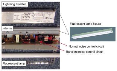
1. Electromagnetic environment surrounding communications facilitiesThe proliferation of broadband services has made access to the Internet easy for ordinary households as well as businesses. That trend is bringing about the connection of various electrical and electronic devices known as household appliances to networks and the distribution of various kinds of data via the Internet. For that purpose, various kinds of high-speed communication techniques that use metallic wires have been developed and the signals transmitted over them have higher and higher frequencies. On the other hand, short-range wireless communication techniques have been developed toward the ubiquitous society, and technology that uses even higher frequency bands is appearing. Furthermore, rising concern about environmental problems is leading to the introduction of inverter technology and other such measures to reduce electric power consumption in homes. Thus, the communication environment is changing dramatically, and at the same time the circumstances surrounding communication systems are also changing greatly. For that reason, the communication environment is becoming more complex, and at the same time the electromagnetic environment is also increasing in complexity. Accordingly, new EMC (electromagnetic compatibility) problems are arising with the development of this new communication technology, and research and development of technology for solving those problems is becoming more important. NTT Environment and Energy Systems Laboratories is taking up various challenges toward solutions of EMC problems. We are also trying to develop new business that applies the EMC technology we have accumulated so far. In this article, we describe a low-noise fluorescent light, a shielded data vault, and an electromagnetic sensor as examples of products for business development making use of EMC technology. 2. Low-noise inverter-type fluorescent lampHome electronics devices and fluorescent lamps and other lighting products that are equipped with inverter technology are being widely sold on the market. Switching to inverter-type fluorescent lamps in particular is considered to be an energy conservation means to address environmental concerns. While such lamps are energy efficient due to electric power control, they sometimes generate electromagnetic interference (EMI) because the inverter operates at a high frequency. For that reason, hospitals may restrict the use of inverter-type fluorescent lamps in computer rooms and other environments containing equipment that is sensitive to EMI to prevent harmful effects from the EMI emitted by them or may take measures to prevent such effects. By applying our accumulated EMC technology to these inverter-equipped fluorescent lamps, we have developed a better lamp that generates less noise [1]. Inverter-type fluorescent lamps have an electronic stabilizer that controls the switching at frequencies higher (several tens of kilohertz or more) than the commercial power supply (50 or 60 Hz), so while they are small and save energy (usually about 30%), the transient current noise generated when the lamp is turned on or off and the normal radiation noise are a greater problem than with conventional rapid-start-type fluorescent lamps and electric-starter-type fluorescent lamps. Therefore, we developed a new filter circuit that can suppress both transient current noise and normal noise and integrated it into the inverter circuit of the electronic stabilizer. This solves the noise problem at low cost while preserving the energy conservation effect (Fig. 1). In addition to the EMI filter for suppressing normal noise, a MOSFET (metal oxide semiconductor field effect transistor) is used to achieve a gradual transition in the load impedance on the bias circuit to suppress the inrush voltage and current fluctuation that occur when the power supply is switched on or off.
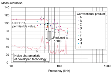
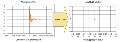
The result is that the original energy efficiency of the inverter circuit is retained, but there is much less noise than with a conventional high-frequency inverter. Compared with the conventional rapid-start fluorescent lamp, the new lamp has an energy efficiency of 28% and both the transient current noise and normal noise are reduced by about 99%. We have thus achieved a result that is far less than the value permitted by international standards (CISPR 15) for conductive interference normal noise of 150 kHz or less (Figs. 2 and 3).
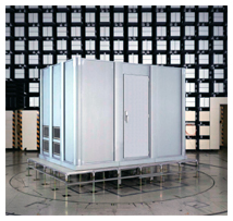
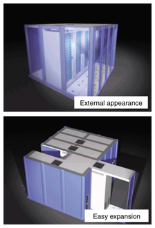
This low-noise inverter-type fluorescent lamp makes it possible to introduce energy-efficient lamps into environments where EMI problems have prevented the use of conventional inverter-type fluorescent lamps. Furthermore, by combining this technology with small-diameter (15.5 mm) high-luminance fluorescent lamps, we have achieved a long life and energy efficiency (50%) and made lighting that is also environmentally friendly with respect to manufacture and disposal [2]. 3. iDC shielded vaultAs important data such as personal information and electronic settlements circulates and accumulates on networks, data center security is year-by-year becoming an important issue. In particular, the need for physical security is increasing as the importance of information increases. Problems in this respect include the theft of important data via electromagnetic radiation leaking from servers in data centers (as highlighted by TEMPEST*) and electromagnetic radiation attacks, which use strong electromagnetic radiation near the data center to damage the system or interfere with its operation. As the ubiquitous society moves forward, the use of portable and compact wireless devices within data centers will probably increase. The daily use of wireless devices in the vicinity of important data equipment (e.g., servers) makes it essential to protect the equipment from malfunctioning as a result of the electromagnetic fields produced by those devices. One means of protecting equipment from electromagnetic radiation leakage and external sources of electromagnetic radiation is electromagnetic radiation shielding. However, if such shielding is installed at existing data centers, expandability is difficult and the time from design to the completion of construction is long and involves a high cost. Under such circumstances, we have applied the EMC countermeasure technology and electromagnetic radiation security evaluation and countermeasure technology that we have developed so far to establish practical techniques for constructing electromagnetic radiation shielded rooms in response to the demand for high security in data centers. One such development is the “iDC shielded vault” [3]–[5] (Fig. 4).
The iDC (Internet data center) shielded vault is based on 19-inch cabinet racks, which are typical in data centers and server rooms. It can withstand an earthquake intensity of 6 on the Japanese seven-point seismic scale without collapsing. Use of a simple metal panel joining method produces an electromagnetic radiation shielded room that has a shielding factor of 50 dB or more, yet it is light and inexpensive. Including the construction cost, it can be made for from 1/2 to 1/5 the cost of existing methods. The number of racks can be changed to accommodate changes in the number of machines, which ensures easy expandability—something that has previously been difficult for shielded rooms. The double-door construction guarantees that rack doors can be opened and closed while maintaining higher shielding performance than previous room facilities. That construction also prevents electromagnetic leakage and electromagnetic attacks during maintenance work (Fig. 5). A security cabin (private room) can also be created by adding locks.
The application fields include adding to the electromagnetic shielding choices for existing data centers whose purpose is to protect important information, as typified by PKI (public key infrastructure), credit, and electronic transaction data; for the construction of an electromagnetic radiation shield in the customer’s data center or server room; and for the construction of server rooms in environments where the electromagnetic environment is tending to deteriorate, such as offices and factories. Furthermore, this technology can be applied directly to small-scale shielded room construction, so possible applications include experimental chambers for the wireless technology that is necessary for the development of ubiquitous communication devices and ubiquitous-ready offices and other locations where the use of many wireless devices is expected.
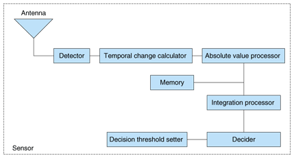
4. Security sensors that use electromagnetic wave antennasIn recent years, increases in home intrusion and other trespassing crimes have increased the need for security services. Methods that use infrared radiation are popular for intrusion detection, but the body heat of pets and high room temperatures can cause false detection, so this method cannot be used in all situations. One proposal for an intrusion detection method is to utilize the radio signals from cell phone base stations and other such electromagnetic radiation that are already present all around us. Human movement causes fluctuations in the signal voltage received at an antenna [6]. This does not need a source for generating new electromagnetic waves, so it has the advantages of having no effect on the surrounding electromagnetic environment and being applicable in places where infrared methods are problematic because it is temperature-independent. However, the received signal voltages of cell phone base station signals and other such electromagnetic waves are not always stable: there can sometimes be changes in the external environment that cause sharp fluctuations over very short time periods. Accordingly, a disadvantage of this method is that if detection is based simply on abnormalities in the time difference of the received signal voltage fluctuation, detection errors may arise as a result of environmental factors. We have devised a detection method in which the temporal fluctuation in the received signal voltage is further integrated over a constant time interval to extract a quantity that is characteristic of human intrusion, and we are studying its practical implementation [7]. The configuration of the electromagnetic wave sensing method is shown in Fig. 6. First, the amount of temporal change in the detected antenna received signal voltage is calculated at constant time intervals, and its absolute value is computed. To distinguish between the sharp fluctuations caused by environmental factors and fluctuations caused by human intrusion, we make use of the fact that the duration of the received signal voltage fluctuation caused by human movement is sufficiently longer than environmentally induced fluctuation. In our method, the amount of temporal change is integrated over fixed time intervals. That method extracts only the received signal voltage fluctuation due to human intrusion.
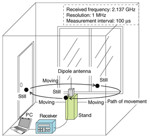
The measurement environment and the measurement apparatus used to test the applicability of this method are illustrated in Fig. 7. Experiments were conducted in a 5-m3 conference room with a dipole antenna placed at the center of the room. A person moved in the space around the antenna and the fluctuation in the voltage of the signal received by the antenna was detected and integrated by a receiver and a personal computer. For the received signal that was measured, we used the radio signal of an NTT DoCoMo FOMA cell phone service base station.
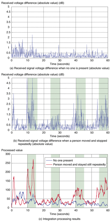
The measurement results are presented in Fig. 8. The graphs show the absolute values of received signal voltage difference: Fig. 8(a) is for when no one was present and Fig. 8(b) is for when a person repeatedly moved and remained still for constant time intervals. The green shading in Fig. 8(b) indicates the time periods when the person was moving. Comparison of these results reveals that the received signal voltage difference was large during human movement in Fig. 8(b), but in Fig. 8(a) the received signal voltage difference is sometimes large even in the periods of no movement. This indicates the difficulty of distinguishing between human presence or absence simply by means of the fluctuation in received signal voltage. The results of applying the integration processing to the data presented in Figs. 8(a) and (b) are shown in Fig. 8(c), where the blue lines represent the data for when no person was present and the red lines represent the data for when a person repeatedly moved and stayed still. Comparing these, we can see a strong correlation between the processed value and human presence.
These results show that our method can reduce the probability of detection errors caused by the external environment. In future work, we will investigate ways to set the threshold value, which is important in the detection process. We will also continue investigating new sensor technology with the aim of developing new business in the field of security. 5. ConclusionThe Electromagnetic Environment Technology Group of NTT Environment and Energy Systems Laboratories is making use of the EMC technology relevant to electromagnetic radiation that has already been accumulated to develop technology for new fields such as security. We are also taking up the challenge of turning research and development results into commercial business. References
|
||||||||||||||||||||||||||