|
|||||||||||||||||||||||||||
|
|
|||||||||||||||||||||||||||
       |
Selected Papers: Quantum Computing Vol. 6, No. 1, pp. 37–41, Jan. 2008. https://doi.org/10.53829/ntr200801sp4 Quantum Information Devices Using Semiconductor Quantum DotsAbstractRecent developments in the control and measurement of single electrons enable us to search for electron dynamics in semiconductor quantum dots. Quantum computing may become realistic as a result of a deep understanding of nanometer-scale semiconductor physics and the development of quantum information devices. This paper describes some recent progress in quantum information devices and discusses the direction of this research. 
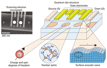
1. Controlling single electronsDevelopments in modern electronics have been made through the progress of transistors, which control an electric current. Nanometer-scale devices accommodate only a small number of electrons, which has led to the emergence of quantum mechanical characteristics of the electron dynamics. Single-electron devices, whose transport characteristics are modified by a single electron, can be fabricated by nanolithography and are interesting for low-power devices [1]. Moreover, the quantum electron dynamics of one electron or a few electrons in such devices can be used to develop quantum information devices for future parallel information processing. Fundamental research in this direction has been conducted in this last decade and is expected to progress in future. NTT Basic Research Laboratories has been researching quantum information devices and time-dependent tunneling phenomena in quantum dots [2]–[4]. A typical quantum dot (double quantum dot) device fabricated using high-quality crystal growth (molecular beam epitaxy) and a nanofabrication technique (electron beam lithography) is shown in Fig. 1. The device has five metal gate electrodes between the source and drain electrodes; these are used to change some important parameters of the quantum dots. Various types of physical analysis have been performed with high-frequency measurements.
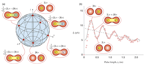
For instance, molecule-like bonding states (ionic and covalent) have been experimentally verified using microwave spectroscopy. The semiconductor charge qubit demonstrated in such a device opened up a pathway to quantum information devices with semiconductors, as discussed later. Recent results indicate that electrons are interacting with their spin degree of freedom as well as with the nuclear spins of the host material (GaAs). High-coherency and various functionalities are expected by combining different types of quanta. Moreover, it is also understood that electrons are strongly coupled to the crystal lattice (bulk phonon and surface acoustic waves). The electron-phonon coupling, which is usually regarded as a source of decoherence, may be utilized in a positive way by treating phonons as a controllable excitation source. Here, I would like to discuss how the electronic characteristics can be designed for quantum information devices. 2. Quantum information devicesQuantum information devices include memories (quantum bits) themselves and related devices for reading, writing, and operating quantum information. These functionalities must be integrated in order to build a large-scale quantum computer. The wave and particle behaviors of single particles (electrons in our case) should be manipulated in quantum information devices. The wave nature is used to achieve constructive interference for a desirable quantum state, and the particle nature is used to digitize the results for readout. Quantum computing is designed to prepare the initial state using the particle behavior, perform information processes using the wave behavior, and read out the final state using the particle behavior. DiVincenzo proposed the following five requirements for building such quantum information devices [1]. These are the abilities to (1) prepare a state in an initial known state, (2) manipulate the state for logical operations in a programmable manner, (3) read out the final state, (4) fabricate a sufficient number of qubits, and (5) maintain the coherency of the system until the end of the required processing. Quantum information devices are generally discussed in terms of how well these criteria can be met [2]. 3. Development of charge qubitsA semiconductor charge qubit in a double-dot device (see Fig. 1) is based on a two-level system with an electron occupying the left dot state (|L>) and the right dot state (|R>) [4], [6]. Although these two choices are requested classically, quantum mechanics allows us to prepare the system as a linear superposition of the two states. Any superposition can be represented at points on the Bloch sphere shown in Fig. 2(a). In addition to the classical states at the North Pole (|L>) and South Pole (|R>), a superposition is identified by the latitude for the occupation probability and the longitude for the phase difference.
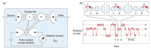
The superposition of a charge qubit can be prepared by using high-speed electrical pulses [2]. The experimental data in Fig. 2(b) shows the current proportional to the occupation probability for the left dot state (|L>) after the application of an electric pulse (period tp) for resonant tunneling. The oscillation pattern suggests an electron coherently moving back and forth between the two dots, and the latitude (occupation) of the state can be controlled via the pulse period. We have also demonstrated that the longitude (phase) can also be controlled by tailoring the pulse shape. We expect to make a two-qubit system by fabricating two double quantum dots in close proximity to each other. We have experimentally confirmed significant electrostatic coupling between two double quantum dots, which is encouraging for the demonstration of two-qubit operation [7]. 4. Precise charge detectionThe experimental results mentioned in the previous section (Fig. 2) were obtained by measuring the current from millions of identical coherent oscillations (ensemble measurement). This is because a current meter requires millions of electrons to achieve detection. However, single-shot measurement, in which a state is measured after each coherent oscillation, is strongly desired for better quantum information devices. A schematic of a circuit that measures the flow of a single electron through a double quantum dot between source and drain electrodes is shown in Fig. 3(a) [8], [9]. The motion of an electron is detected with a point-contact charge sensor, which is capacitively coupled to the left and right dots asymmetrically. A tunneling barrier in the point contact is influenced by the dot charge, so the point contact works as a charge sensor. Figure 3(b) shows the changes in detector current among three levels, measuring individual tunneling processes in the double quantum dot, as illustrated in the insets.
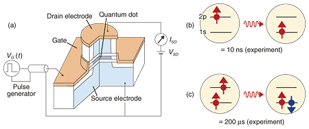
This single-electron counting device actually measures when and in which direction a single electron has flowed and acts as a sensitive current meter. Moreover, a statistical analysis of electrical current (counting statistics) reveals correlated transport in a nanostructure. We expect that such devices will be useful in developing nanoelectronics or molecular electronics, in which the analysis of a small current is essential. The counting device is also useful as a single-shot readout for a charge qubit. The device in Fig. 3(a) may be regarded as a charge detector directly coupled to a charge qubit. High-speed charge detection would allow single-shot read out for the qubit. 5. Electron and nuclear spinsAlthough a charge qubit has advantages for high-speed quantum operation within a nanosecond and for the expected single-shot measurement, as mentioned in the previous sections, a drawback is its relatively short decoherence time. Electron spins and nuclear spins are expected to have longer decoherence time and may be useful for quantum information storage. We have developed an electrical pump-and-probe technique for investigating the relaxation time of orbital and spin degrees of freedom and succeeded in establishing some spin-related selection rules in the relaxation processes. A schematic illustration of the device is shown in Fig. 4(a). A voltage pulse is applied to the gate electrode to inject an electron to an excited state (pump) and selectively extract it from the excited state (probe) after various waiting times. The relaxation time can be obtained from the pump-probe technique [10], [11].
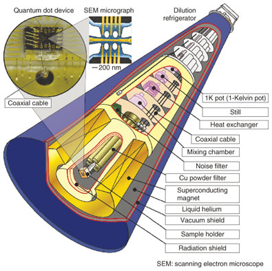
For a one-electron quantum dot, the first excited state (2p state) relaxes to the ground state (1s state) within a short time of about 10 ns (Fig. 4(b)). In contrast, for a two-electron quantum dot, relaxation from the spin-triplet excited state to the singlet ground state has a much longer relaxation time (a few hundred microseconds) owing to the spin selection rule (Fig. 4(c)). The observation of such a long spin lifetime has actually led to various experiments on electron spin dynamics in quantum dots. Nuclear spins, which have much longer relaxation times, are promising for quantum information memories. The recent understanding of hyperfine coupling between electron and nuclear spins may be used to exchange quantum information between different particles. 6. Cryogenic techniquesA low-temperature, low-noise environment is essential for studying quantum effects in semiconductor nanostructures. A schematic of a dilution refrigerator, which can provide temperatures below 0.01 K by continuously circulating 3He, is shown in Fig. 5. High-frequency superconducting coaxial cables, copper powder filters, and noise filters are important experimental techniques for studying low-noise measurement. Further progress in quantum information devices can be obtained by developing low-temperature and low-noise techniques.
7. ProspectsIn this paper, I have discussed the basic elements of quantum information processing, e.g., initialization, coherent manipulation, and (single-shot) measurement, on semiconductor devices with examples from recent experiments on semiconductor physics. Large-scale integration techniques are also desired for quantum information devices. However, quantum information interfaces between different quantum systems will be more important for utilizing the different advantages of various systems. A deep understanding of semiconductor physics is required in order to develop quantum information technology. References
|
||||||||||||||||||||||||||