|
|||||||||||||||||||
|
|
|||||||||||||||||||
       |
Selected Papers: Quantum Computing Vol. 6, No. 1, pp. 42–46, Jan. 2008. https://doi.org/10.53829/ntr200801sp5 Nuclear-spin-based Quantum Information Devices in Solid-State Nanometer-Scale StructuresAbstractWe describe our recent research on quantum information devices that use nuclear spins, which are the very tiny magnetic moments possessed by nuclei. Since nuclear spins can hold quantum information for a long time, they are expected to be used for quantum bits. In this paper, we report on our success in controlling and detecting nuclear spins in semiconductor nanometer-scale structures. 
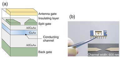
1. IntroductionThe prospect of making conceptually new devices that make use of the principles of quantum mechanics is attracting considerable interest in modern physics. A quantum computer is a good example. It utilizes the superposition of quantum states, allowing parallel computation for an infinitely large amount of data. This parallel computation could mean that quantum computers will have the potential to solve certain types of problems much faster than the fastest classical computer. A quantum computer uses quantum bits (qubits). Unlike a classical bit, which can represent either “0” or “1”, a qubit can represent “0”, “1”, or a superposition of them. Here, we use the notation |0> and |1> for the “0” and “1” states of a qubit, respectively. The superposition state is described as α|0> + β|1> (|α|2 + |β|2 = 1). In principle, any quantum two-state system can be a qubit. One possible candidate is a nuclear spin system. Since nuclear spins have the significant advantage of a long coherence time, which shows how long qubits can retain quantum information, they are expected to be used for a quantum memory. Note that in a nuclear-spin qubit, |0> and |1> correspond to nuclear spins pointing in the down and up directions, respectively. In this paper, we report demonstrating the control of nuclear spins in semiconductor nanometer-scale structures. This will allow us to integrate nuclear-spin qubits in a semiconductor. 2. Experiment2.1 Device structureA cross section of the device is shown in Fig. 1(a) [1], [2]. The device consists of a 20-nm-thick GaAs/Al0.3Ga0.7As quantum well structure grown on a GaAs (001) substrate. A pair of metal electrodes forming a single split gate with a gap of 600 nm was deposited on the surface, as shown by the scanning electron microscope (SEM) image in Fig. 1(b). When a negative bias of -0.4 V was applied to the split gate, the conducting two-dimensional electron gas confined in the quantum well was squeezed into a narrow channel with a width of less than 600 nm. As described below, the spins of the 69Ga, 71Ga, and 75As nuclei in the narrow channel could be polarized. An antenna gate was deposited just above the split gate. By applying a high-frequency current to the antenna gate, we were able to apply radio frequency (RF) pulses to the narrow channel in order to control the nuclear spins. The device was mounted on a chip-carrier (Fig. 1(b)) and placed in a cryostat.
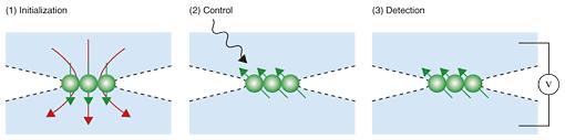
2.2 Experimental techniqueThe experimental procedure for controlling nuclear spins in the nanometer-scale region is shown in Fig. 2. (1) At low temperature (about 100 mK), when the electrical system is set to a special state called the fractional quantum Hall state by applying a static magnetic field (B ≈ 5 T) perpendicular to the sample, a current induces flip-flop scattering between electron and nuclear spins. When the current is sufficiently large, nuclear spins are polarized [3], [4]. In our device, this occurs only when a certain negative bias (about -0.4 V) is applied to the split gate and the current exceeds a threshold. Owing to the narrow constriction, the local current density exceeds the threshold only in the channel, thereby locally producing nuclear polarization. As a result, the nuclear spin state is initialized to |0>. (2) The antenna gate applies an RF pulse to the polarized nuclear spins. When the frequency, amplitude, and width of the RF pulse correspond to certain values, the nuclear spins flip to the other direction and the state becomes |1>. When the amplitude or width of the RF pulse is half that required to flip the nuclear spins, the spins rotate to the middle, where |0> and |1> are superposed with a ratio of 1:1. The superposition state is described as (1/2)1/2(|0>+|1>). Similarly, by tuning the parameters of the RF pulse, we can obtain an arbitrary superposition state α|0> + β|1>. (3) Since the nuclear spins interact with electron spins, the nuclear spin polarization affects the electronic state and hence the resistance of the system. As a result, the nuclear spin polarization in the superposition state |β|2 - |α|2 is detected from the change in resistance ΔRxx. The sensitivity of this resistive detection technique is more than three orders of magnitude higher than that of the conventional technique for detecting nuclear magnetic moment by using coils.
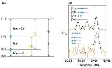
3. Demonstration of qubit operations3.1 InitializationNow we present some experimental results for controlling 69Ga, 71Ga, and 75As nuclei, which form four energy levels. As shown in Fig. 3(a), the four levels can be treated as an effective two-qubit system by regarding them as |00>, |01>, |10>, and |11> from lower energy, respectively. In |01>, for instance, the first qubit is in |0> and the second qubit is in |1>.
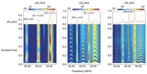
Before qubit operations, the system must be initialized. In a one-qubit system consisting of |0> and |1>, as described in Sec. 2.2, adequate initialization can be achieved by polarizing the nuclear spins by applying a current. In a two-qubit system, however, the current-induced nuclear spin polarization is insufficient for the initialization. Even after polarization, the nuclear spins are distributed among the four levels. Their occupation ratio is largest in |11> and decreases gradually with decreasing energy (upper panel in Fig. 3(a)). As RF pulses are applied to equalize the occupations in |00>, |01>, and |10>, the occupation in the three levels becomes constant, while that in |11> remains large (lower panel in Fig. 3(b)). Such a system is called an effective pure state and can be used as an initial state for qubit operations. Note that a system with all nuclear spins in |11> is called a pure state. The effective pure state can be treated mathematically in the same way as the pure state. 3.2 Creation of a superposition stateNuclear spin states can be controlled by the irradiation of RF pulses. The ΔRxx as a function of RF frequency and pulse duration is shown in Fig. 4. When the energy of the RF pulse, which is proportional to the RF frequency, corresponds to the energy difference between adjacent nuclear spin levels, the nuclear spins rotate between the two levels. The rotation is detected as an oscillation of ΔRxx. The oscillation on the right-hand side of Fig. 4(a) corresponds to a nuclear spin rotation between |11> and |10>. The oscillations in the center and on the left-hand side correspond to rotations between |10> and |01> and between |01> and |00>, respectively. As the power of the RF pulse is increased, the frequency of the ΔRxx oscillations increases. More importantly, two slow oscillations appear between the three oscillations (Fig. 4(b)). The slow oscillations are assigned to nuclear spin rotations between |01> and |11> and between |00> and |10>, as indicated by orange arrows in Fig. 3(a). When the RF power is increased further, a narrow peak appears in the center oscillation (Fig. 4(c)). This peak is assigned to the transition between |00> and |11> (green arrows in Fig. 3(a)). These results indicate that, starting from the initial state |11>, we can create an arbitrary superposition state of any combination between two of the four levels.
The ΔRxx oscillations decay with a time constant of about 1 ms. This decay time, called the coherence time, represents how long the superposition state, and hence quantum information, is maintained. The value of 1 ms is several orders of magnitude longer than those reported for other solid-state qubit systems (1 ns to 1 µs). Furthermore, the coherence time can be extended several fold by decoupling interactions between nuclei and their environment [5]. 3.3 Logic gate operationsBy using the operations described in Sec. 3.2, we can demonstrate two-qubit logic gates. For instance, by applying RF pulses to exchange the nuclear spin state between |00> and |01> and between |10> and |11>, we made the second qubit rotate from |0> to |1> while keeping the first qubit fixed. This operation corresponds to a NOT gate. We achieved SWAP and CNOT gates through operations that exchange |01> for |10> and |10> for |11>, respectively. Here, a SWAP gate swaps two qubits without using any control inputs and a CNOT (controlled NOT) gate flips the second qubit (the target qubit) if and only if the first qubit (the control qubit) is 1. 4. ConclusionIn conclusion, we have demonstrated two-qubit operations on nuclear spins using a nanometer-scale semiconductor device. The fabrication of the device using semiconductor fine patterning techniques shows the potential scalability of nuclear-spin qubits. Moreover, the long coherence time of the order of 1 ms is a significant advantage of this device. We believe that our experiments will stimulate further work on fabricating a nuclear-spin-based solid-state quantum computer. AcknowledgmentsWe thank G. Yusa, K. Hashimoto, and Y. Hirayama of Tohoku University for useful discussions. References
|
||||||||||||||||||