|
|||||||||||||||||||||||||||
|
|
|||||||||||||||||||||||||||
       |
Special Feature: Applied Technology for Millimeter and Terahertz Electromagnetic Waves Vol. 7, No. 3, pp. 11–16, Mar. 2009. https://doi.org/10.53829/ntr200903sf2 Compact, Low-power, 120-GHz-band Wireless Link for 10-Gbit/s Data TransmissionAbstractThis article introduces a compact, low-power, 120-GHz-band 10-Gbit/s wireless link that can be used in various situations. The size and power consumption of the transmitter and receiver module have been reduced by using an indium-phosphide high electron mobility transistor microwave monolithic integrated circuit. A license for testing this link was obtained in January 2007, and field testing at 10 Gbit/s was successful over a distance of 800 m. 
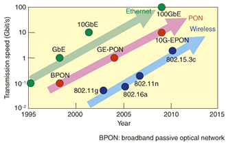
1. IntroductionThe data capacity required for the exchange of data, distribution of high-definition video, and other services being developed on the Internet continues to rise each year and the communications services that handle this traffic continue to expand accordingly (Fig. 1). In 2004, regulations were set for GE-PON (Gigabit Ethernet passive optical network), which provides 1-Gbit/s services based on the PON technology used for access lines, making way for 1-Gbit/s lines to individual homes. This expansion will continue with the approval of 10G EPON (10-Gbit/s Ethernet PON), providing 10 Gbit/s as a PON standard, and the standardization of 100GbE (100-Gbit/s Ethernet) expected by the year 2010.
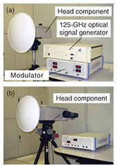
For areas where, for cost or geographic reasons, it is difficult to install physical lines, high-speed wireless systems can be used as an alternative. Wireless systems are also useful for setting up temporary connections to handle loads at times of disaster and special events or for other reasons. However, current wireless technologies are limited to transmission speeds of a few hundred megabits per second, and standardization of 802.15.3c wireless, scheduled for 2010, for 60-GHz-band wireless systems will increase this to only a few gigabits per second. Thus, there is a need for ultrafast wireless technology that can support network standards like 10GbE and 10G EPON, on which new services will be developed. In the broadcasting field, the switch from analog to digital broadcasting will be completed by 2011 in Japan, and the need for wireless technology to transmit high-definition (HD) video content is increasing. However, HD video requires up to 1.5 Gbit/s, and the lack of wireless technology able to transmit multiple HD camera feeds from a live broadcast site is becoming a problem. NTT Microsystem Integration Laboratories previously developed a 120-GHz-band millimeter-wave wireless link to resolve these problems [1], [2]. It uses the ultrahigh-frequency 120-GHz band to achieve 10-Gbit/s data transfer. In addition to providing support for 10-Gbit/s-class communications, it can be used to transmit up to six multiplexed HD video signals, so its practical implementation as a video feed for on-site live broadcasting is much anticipated. The so-called millimeter-wave band from 30 to 300 GHz has not yet been fully exploited commercially, so there is increasing demand to develop it to reduce congestion below 30 GHz [3]. There are still very few devices that operate in the over-100-GHz range in particular, so wireless communications technology in this range is receiving attention. A millimeter-wave wireless link we developed earlier is shown in Fig. 2. It generates a 120-GHz signal with 10-Gbit/s wideband modulation by using optical device technology. A 125-GHz modulated signal is generated in the transmitter as an optical signal by a 125-GHz optical signal generator and 10-Gbit/s modulator. It then undergoes photoelectric conversion by a uni-traveling carrier photodiode [4] in the transmitter head, which allows output as a 120-GHz-band, 10-Gbit/s millimeter-wave modulated signal. That link was approved for a radio test license by the Ministry of Internal Affairs and Communications (MIC) in 2005, and soon afterwards, we demonstrated the world’s first successful, error-free transmission of 10 Gbit/s wireless signals over a distance of 200 m in field testing.
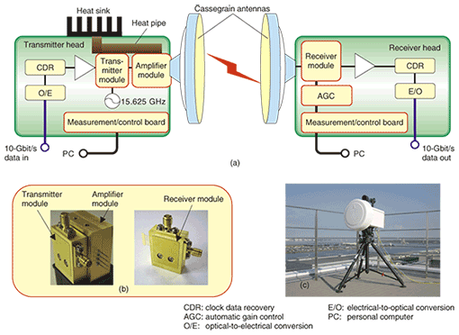
However, compared with existing portable wireless systems, the size and power consumption of this equipment was too large to be practical. Although optical device technology enabled the generation and modulation of an over-100-GHz signal, optical devices are generally larger and require more power than electronic ones. This presented significant problems for use at disaster sites or for on-site reporting, where wireless systems must have good portability and a long battery life. Moreover, to enable the transmission characteristics to be tested under various weather conditions and in various locations, the size and power consumption of the wireless link must be reduced. Thus, we are continuing to research and develop new 120 GHz-band millimeter-wave wireless links to address these needs. Significant size and power-consumption reductions are targeted, and to enable operation in various situations and for long periods of time, we are placing particular emphasis on improving resistance to environmental factors and providing support for remote operation and monitoring. 2. DesignThe architecture of an all-electronic millimeter-wave wireless link that we are developing is shown in Fig. 3(a). In this architecture, the most significant difference from the earlier link is that a 120-GHz-band transmitter and receiver module [5], [6] (Fig. 3(b)) with an indium-phosphide high electron mobility transistor microwave monolithic integrated circuit (InP HEMT MMIC) developed by NTT Photonics Laboratories is used to generate and modulate the millimeter-wave signal. The earlier link also used an MMIC to amplify and detect the millimeter-wave signal, but since then, high-speed semiconductor technology and high-frequency design and implementation technology have advanced, allowing all of the 120-GHz-band analog processing in this link to be accomplished on a single MMIC. The 10-Gbit/s signal is input to the transmitter head via an optical fiber and passed to the transmitter module through optoelectronic converter, clock data recovery, and amplifier circuits. The transmitter module generates a 125-GHz signal by applying an eight-times frequency multiplier to a 15.625-GHz signal output by an external oscillator. This signal is amplitude-modulated using the 10-Gbit/s data signal and then output. The 125-GHz modulated signal from the transmitter module is amplified by an amplifier module and emitted from a Cassegrain antenna. At the receiver, the signal from the antenna is amplified in the receiver module by a low-noise amplifier, and the 10-Gbit/s data signal is demodulated using an envelope detector. An external view of the all-electronic millimeter-wave wireless link is shown in Fig. 3(c). Whereas the earlier system (Fig. 2) with its mixture of optical and electronic devices required two cabinets to generate and modulate the 120-GHz signal, the new link performs all of the analog processing on a single MMIC with a size of only a few square millimeters. The transmitter module incorporating this MMIC occupies only about 10 cm3, so we were able to greatly reduce the size of the analog processing section. As a result, all components required for wireless transmission could be placed in the head-component behind the antenna, allowing us to further improve the link’s portability. Another major improvement is that power consumption for generating and modulating the 120-GHz-band signal using the MMIC is much lower than that of the earlier link. The new link requires about 60 W for the transmitter (and 40 W for the receiver)—a reduction in transmitter power consumption of about 65% compared with the earlier link. This enables the transmitter to operate for long periods of time on battery power and greatly increases its range of possible operating locations.
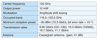
The new link was created to measure 120-GHz-band transmission characteristics in various environments, so good resistance to environmental factors was required. The head section was made airtight, and a double-wall structure was used to improve resistance to rain, dust, and overheating caused by direct sunlight. However, this solid construction isolates the internal components from the outside air, which is a disadvantage for cooling. To resolve this, we used a lightweight heat pipe with excellent thermal conductivity to thermally connect the millimeter-wave module to an external heat sink, using thermal design techniques to improve the link’s heat resistance. Furthermore, to facilitate transmission over various distances automatically, we implemented automatic gain control for the receiver’s amplifier to make appropriate adjustments according to the received signal power and avoid distortion caused by excessive input signal levels. We also equipped the transmitter and receiver with control boards having a central processing unit, memory, network interface, and instrumentation board in anticipation of use in long-term, on-going experiments to gather and store data for later analysis of the transmission characteristics of millimeter-wave signals. An external terminal can be connected to the control board to remotely control the wireless device for convenience and ease of operation. The instrumentation board allows automatic measurement of the voltage and current to each device, temperature, humidity, received signal power, and other parameters; these can be output to an external personal computer from the onboard memory. 3. ExperimentsThe specifications of the compact, low-power millimeter-wave wireless link are listed in Table 1. The new link produces a 120-GHz modulated signal of quality comparable to that of the earlier link and achieves an increase in sensitivity of 5 dB through improvements to the receiver MMIC. The maximum possible transmission distance is estimated to be about 2 km, on the basis of the output power, antenna gain (Cassegrain antenna: 51 dBi), and required minimum received signal power. A license for testing this link was obtained from the MIC in January 2007, and field testing performed in collaboration with Fuji Television successfully achieved error-free transmission (bit error rate: less than 10-12) at 10 Gbit/s over the distance of 800 m between Fuji Television’s headquarters and their new studio.
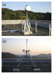
To make the wireless link practical, we need to understand its transmission characteristics under a variety of environmental conditions so that technicians can set up reliable connections. However, the transmission characteristics of 120-GHz-band signals are affected by rain, snow, fog, and other weather conditions, and although we have attenuation estimates based on theoretical computations using techniques like first-order scattering models, not much real data is available yet. For this reason, starting in February 2008, we began continuous, long-term observations of 120-GHz-band transmission characteristics using this link over a distance of 400 m on the roof of the Atsugi Laboratory (Fig. 4(a)). Weather monitoring equipment (Fig. 4(b)) was also set up near the wireless link to measure the temperature, humidity, wind speed, precipitation, and other parameters at one-second intervals for time-synchronized comparison with the received signal power.
4. Future developmentsTo increase the transmission range and carrier-to-noise ratio of future wireless links, we hope to increase the transmitter power and receiver sensitivity. We will also study communications methods and develop new devices and system designs to increase channel capacity. We would also like to advance the analysis of the propagation characteristics of 120-GHz-band, millimeter-wave signals, particularly their weather dependency, by utilizing data from long-term, continuous transmission tests. AcknowledgmentThis research was partially done under an MIC contract under the “RF Resource Use R&D” initiative. References
|
||||||||||||||||||||||||||