|
|||||||||||||||||||||||||||||||||||
|
|
|||||||||||||||||||||||||||||||||||
       |
Special Feature: Nanobiotechnology Research Vol. 7, No. 8, pp. 30–35, Aug. 2009. https://doi.org/10.53829/ntr200908sf6 Nanometer-scale Analysis of Single MoleculeAbstractIn this article, we describe some of our recent results concerning nanometer-scale analysis. Understanding structural and electrical properties at the single molecule level is vital for molecular electronics, which is a promising candidate for replacing silicon technology. Moreover, the characterization of individual molecules provides us with a lot of useful information about the development of bulk materials. 
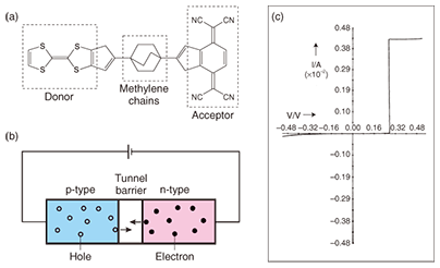
1. IntroductionIndustrial technology based on silicon has developed greatly with the progress in device integration techniques. However, the current lithographic technique is predicted to reach its fundamental limit in the near future if silicon devices continue to decrease in size at the current rate. In addition, there will be inevitable roadblocks caused by fundamental physical constraints such as charge leakage. Therefore, alternative innovative technologies must be considered instead of the traditional silicon technology. Molecular devices (molecular electronics) are a promising candidate. Molecular devices are based on replacing wires, diodes, transistors, and other basic electronic elements used in silicon devices by single molecules or small groups of molecules. Since an individual molecule is at most several nanometers in size, molecular devices are in principle expected to have integration densities that are several orders of magnitude higher than silicon devices, and hence higher operating speeds. To the best of our knowledge, the first report on molecular devices was a theoretical work on a molecular rectifier published by Aviram et al. in 1974 [1]. They proposed the model molecule shown in Fig. 1(a). This molecule is composed of an electron-donor moiety, tetrathiafulvalene (TTF), and an electron-acceptor moiety, tetracyanoquinodimethane, interconnected by methylene bridges. This structure is a molecular analogue of a p-n junction device (Fig. 1(b)). Indeed, the authors calculated the theoretical current-voltage (I-V) characteristics for this molecule and predicted the rectification behavior (Fig. 1(c)). Although their prediction has not yet been realized, their contribution is very significant as a first step toward a molecular device.
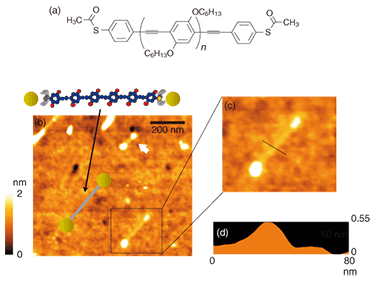
Despite considerable efforts recently, the field of molecular device is still in its infancy. To create molecular devices, it is vital to investigate the properties of individual molecules, which involves measuring the physical properties and observing molecular structures at the single molecule level. This is one of the most difficult and important problems to be solved. How can we isolate just one molecule from a huge number: on the order of 1023? How can we connect wires to such tiny molecules? Since we have no reliable answers to these questions, we must approach this topic via the intrinsic nature of individual molecules. It should be mentioned that even when we handle bulk materials, it is essential to know the properties of individual molecules because the physical properties depend strongly on the molecular shapes and arrangements in solids. In other words, we could design and synthesize molecules with the desired functions and properties because the structures of organic molecules can be finely tuned by organic synthesis. In this article, we introduce these topics using our recent results. 2. Molecular wireAs mentioned above, molecular electronics can be defined as technology that utilizes single or small groups of molecules to construct electronic circuits. We are undertaking a comprehensive investigation ranging from molecular design and development to the characterization of transport properties. In this section, we introduce our recent results related to molecular wires utilizing conducting polymers. With respect to wiring using single molecules, impressive progress has been made on low-molecular-weight materials [2], [3]. However, very few reports have dealt with wiring a polymer into an electrical circuit. There are several possible reasons for this. First, most polymers lack rigidity, which results in self-aggregation leading to the formation of lump-like structures and poor conductivity. Second, the connectivity between polymers and electrodes has not been considered. Non-end-functionalized polymers are difficult to graft to electrodes because such grafting depends on physisorption by chance. Both rigidity and connectivity are indispensable for the formation of good bridges between polymers and electrodes. To overcome these obstacles, we newly designed and synthesized a conducting polymer, poly(p-phenylene ethynylene) (PPE), with thioacetate end-functionalized groups (TA-PPE), as shown in Fig. 2(a) [4]. This polymer has a linear and π-conjugated structure consisting of an alternating combination of acetylene and phenyl rings, so it should be intrinsically rigid and conducting. In addition, the thioacetate end-functionalized group produces selective chemisorption on a gold surface, which makes it easily possible to bridge between gold electrodes. We have been developing such grafting techniques to enable us to characterize polymers at the single molecule level [5], [6]. In this study, we used these techniques to graft PPE to a gold nanoparticle surface as a step toward a molecular device [4]. Topographic images of a hybrid material consisting of TA-PPEs and gold nanoparticles obtained using tapping-mode atomic force microscopy (AFM) on a flat Si(111) surface are shown in Figs. 2(b)–(d). Interestingly, we could clearly observe barbell-like structures, in which a single-polymer chain bridges between two gold nanoparticles. Thus, a PPE offers the ideal rigidity and connectivity vital for molecular wire.
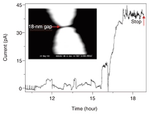
As mentioned above, measuring the transport property at the single molecule level is quite a challenge because of the great difficulty of wiring one or several molecules into a circuit. To accomplish this, we must fabricate electrodes whose separation is comparable to the size of individual molecules (nanogap electrodes). However, it is very difficult to fabricate such electrodes with conventional lithographic techniques since the size of a single molecule is generally less than 10 nm. Developing a method for fabricating nanogap electrodes is currently recognized as one of the most important topics in molecular electronics. In this study, we used an electroplating method that we have developed [7]. This method is simple and controllable and includes the electrochemical deposition of gold on a pair of electrodes, which is halted just before the electrodes make contact with each other. Using this approach, we fabricated gold nanogap electrodes with a gap of 18 nm. If we can successfully achieve a single-molecule bridge between nanogap electrodes, how can we confirm that it is the single target-molecule? We cannot use scanning electron microscopy (SEM) or AFM to detect a single molecule because it would be beyond their resolution limits. Therefore, we developed a new technique to observe a single molecule indirectly. The process of wiring TA-PPE molecules into nanogap electrodes was monitored accurately in situ with a current-time circuit [8]. That is, nanogap electrodes were immersed in a dilute organic solution of TA-PPE (~10–8 M). The current through the nanogap electrodes was monitored by applying a small bias to them. The results are shown in Fig. 3. Before the PPE molecules formed a bridge between the nanogap electrodes, the current did not flow since organic solvent is a good insulator. After 16 hours, we observed a jump in the current indicating that a single polymer was trapped between the nanogap electrodes and had formed a successful connection between them. With careful experimentation, we once observed 19 current jumps during a 130-hour period, corresponding to a connected nanowire with a diameter of around 20 nm. It is very likely that each jump corresponded to a one-molecule connection. Therefore, if the self-assembly process is halted by gently removing the sample from the polymer solution as soon as the first current jump is observed, it should be possible to fabricate a single-polymer junction between nanogap electrodes.
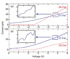
The I-V characteristics of a single-polymer junction measured at room temperature in a vacuum [8] are shown in Fig. 4. It should be mentioned that the current of a pristine nanogap electrode has a finite noise level under the same conditions. Two characteristic features were clearly observed in the I-V characteristics: (i) there was a highly periodic, identical, and repeatable stepwise behavior and (ii) the separation between neighboring steps was around 0.23–0.26 eV. The equidistant steps in the I-V curves cannot be attributed to conductance quantization since the step height is six orders of magnitude smaller than the conductance quantum 2e2/h. We assume that the single-polymer junction could be similar to a quantum dot, in which the terminal sulfur atoms act as two tunnel barriers. First-principles calculations suggest that the stepwise behavior in the I-V curves might be related to resonant electron tunneling. The calculated I-V curves are also shown in Fig. 4 by a red dashed line. The theoretical and experimental results are in good agreement. It should be mentioned that the molecular orbitals of an 18-nm-long TA-PPE are still mainly quantized. Therefore, charge carriers can tunnel through the single-polymer junction only when they have the same energies as the discrete energy levels of the TA-PPE molecular orbitals. Each equidistant step corresponds to the opening of different conducting channels that are associated with the unoccupied molecular orbitals of the PPE molecule. We have successfully demonstrated a quantum transport device utilizing a single polymer. We are still investigating the transport properties using a single low-molecular-weight molecule [9].
3. Single molecule analysis as a useful tool for material developmentIn this section, we introduce the development of novel functional materials based on single molecule analysis. The chemical structure of a newly designed and developed conducting polymer incorporating TTF units in its backbone (TTF polymer) is shown in Fig. 5(a) [10]. TTF and its derivatives have attracted special interest as organic donor molecules that form organic metals and superconductors with various acceptor species despite the fact that organic materials are generally good insulators [11]. In addition, there have recently been several reports that organic thin film transistors (OTFTs) using TTF derivatives exhibit high field-effect mobilities close to that of amorphous silicon [12]. It is well known that strong intermolecular interactions play a crucial role in these attractive electrical properties of TTF derivatives. The TTF polymer has a TTF unit in its polymer backbone, which replaces one of the phenyl rings of four PPE repeating units, and yet it retains a π-conjugated electronic structure. In addition, each polymer terminus is capped with a thioacetyl group to give a good metal/semiconductor interface similar to that of TA-PPE. Thus, the TTF polymer is expected to have rigidity, connectivity, and good conductivity ranging from single-molecule properties to bulk properties.
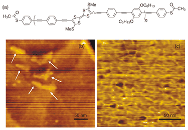
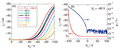
First, we investigated the molecular structure using tapping mode AFM [13]. As shown in Fig. 5(b), in addition to the triangular structures of flat Au(111), we observed rigid rod-like structures typically having a stretched length of 50 nm, a width of 5–10 nm, and a height of 2 nm. This is in good agreement with the average length estimated from 1H-NMR (60 nm) [10]. We assume that the observed structure is a bundle consisting of a few polymers because the heights are slightly large for a single-polymer chain. The TTF polymer maintains its rigidity as expected from its extended π-conjugated structure. In contrast, PPE molecules tend to form an isolated single-chain structure. This difference is presumably due to an enhancement of the intermolecular interaction caused by the introduction of TTF. As the density of the polymer increases (10–1 wt%), each bundle forms a network structure, as shown in Fig. 5(c). Next, we investigated the thin film properties of the TTF polymer [13]. Bottom-contact OTFT devices were fabricated on gold interdigitated array electrodes as source and drain electrodes. A highly doped n-type silicon substrate was used as a gate electrode with a 300-nm-thick oxidized layer as a gate dielectric. Thin films were prepared by slow casting from a 1 wt% toluene solution of the TTF polymer. The output and transfer characteristics of the device are shown in Fig. 6. The device exhibited typical p-type semiconductor behavior with a conductivity of ~10–5 Scm–1, as expected for the electron-donating property of a TTF derivative. The field-effect mobility was estimated to be 6.2 × 10⁻⁶ cm2 V–1 s–1 from the linear region of the transfer characteristic. The on/off ratio was found to be at least 105, which is relatively high for organic semiconductors. To evaluate the effect of introducing a TTF unit, we also characterized OTFTs based on PPE using exactly the same conditions and configuration. The device exhibited p-type semiconducting behavior similar to that of the TTF polymer. However, the field-effect mobility was 4.6 × 10⁻⁸ cm2 V–1 s–1 and the on/off ratio was 103: both these values are about 1/100 of those of the TTF polymer. Since both the TTF polymer and PPE tend to form a rigid rod-like structure, the electronic conduction is mainly attributed to carrier hopping between neighboring polymer chains. In the TTF polymer, widespread sulfur orbitals enhance the intermolecular interaction, resulting in the enhanced OTFT performance. As regards OTFTs, we are also investigating the device performance as the device structure is reduced in size to the nanometer scale [14].
4. ConclusionOur research targets are devices utilizing molecules, which range widely from single molecules to bulk materials such as organic thin film transistors. In both cases, it is very important to understand the intrinsic nature at the single molecule level. We are currently establishing the foundations of molecular electronics. In the near future, we would like to apply our research to nanobiodevices, for example, a highly sensitive sensor for biomolecules such as proteins utilizing the quantum transport properties of a molecular wire. AcknowledgmentsWe thank Dr. Erjing Wang, Professor Hongxiang Li, and Professor Wenping Hu of the Chinese Academy of Sciences for valuable comments and sample preparation. References
|
||||||||||||||||||||||||||||||||||