|
|||||||||||||||||||||||||||||||||||||
|
|
|||||||||||||||||||||||||||||||||||||
       |
Regular Papers Vol. 7, No. 9, pp. 14–23, Sept. 2009. https://doi.org/10.53829/ntr200909rp1 Manipulating Light by Photonic CrystalsAbstractRecent studies of photonic crystals in NTT are reviewed. They have revealed that photonic crystals enable intriguing negative refraction, enormously strong light confinement, and extremely slow light, all of which are impossible to achieve with conventional materials. Owing to these properties, the size and consumption energy of photonic devices, such as optical memories, have been substantially reduced, which opens the door to fully fledged photonic integration. In addition, novel functions arising from photonic crystals may expand the potential of photonics into areas where photonics has not been seriously considered. 
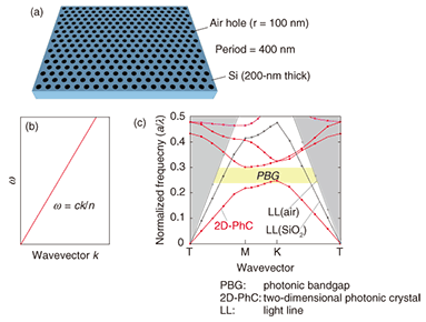
1. What are photonic crystals?It is now well recognized that photonics technologies have been playing a major role in the rapid development of today’s information and communications technology. Photonics has enabled high-speed and wide-bandwidth data handling beyond the limitations of electronics technologies. However, it is also true that photonics is not versatile, and many of the data processing processes still require electronics. For example, memory, logic, and routing functions are still difficult to achieve by photonics alone. This limitation is deeply related to the fundamental properties of light in media. In comparison with electrons in media, it is difficult to confine or store light in a small volume. It is also difficult to control (or change) the speed of light. Moreover, the strength of the light-matter interaction is generally very weak. All of these characteristics severely limit the ways of manipulating light and make photonic data processing more difficult. Photonic crystals are expected to solve these problems by letting us manipulate the behavior of light in media beyond the conventional limitations. This review article explains what a photonic crystal is and what it can do, especially for photonics technologies, and describes NTT’s research activities related to this topic. A photonic crystal is, by definition, an artificially made structure whose refractive index (n) is modulated with a period comparable to the wavelength of light in the material [1]. An example of a photonic crystal is depicted in Fig. 1(a). This is merely a 200-nm-thick silicon (n = 3.46) layer with a two-dimensional array of air (n = 1) holes typically having a radius of 100 nm and a period of 400 nm. These structures can be fabricated by the state-of-the-art semiconductor microfabrication technologies originally developed for integrated electronic circuits, such as complementary metal-oxide semiconductor (CMOS) circuits or dynamic random access memory (DRAM).
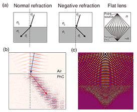
Materials existing in nature show a wide variety of electrical properties, such as conducting, semiconducting, and insulating behaviors. Today’s electronics technologies fully utilize such electrical characteristics of solids. This wide range of electrical properties is attributed to the periodic nature of the atomic lattice for each material. Electrons in the periodic potential form electronic band structures that account for the electrical properties. On the other hand, the optical properties of existing materials are rather limited. The dispersion of light in conventional media, which is given approximately by ω = ck/n (k: wavevector of light, c: speed of light in vacuum (2.998×10⁸ m/s)) is shown in Fig. 1(b). The material properties are included in the refractive index (n), which is normally between 1 and 3.5 and shows little wavelength dependence except around the strongly absorptive region. That is, light behaves in essentially similar ways in different media, in contrast to electrons in different media. This is simply because the periodicity of the atomic lattice is much smaller than the optical wavelength, so the photonic counterpart of the electronic band structure is not formed. The idea of photonic crystals is to artificially introduce periodicity comparable to the optical wavelength in such a way that a photonic band structure is formed. The dispersion of light in a photonic crystal, which exhibits the clear signature of photonic band structure formation, is shown in Fig. 1(c). One of the most important aspects of the band formation is the appearance of the photonic bandgap. This means that this particular photonic crystal behaves like a photonic insulator in the gap wavelength region, where the light propagation is literally inhibited without inducing any absorption loss. In addition, one can significantly change the light propagation even outside the bandgap. In the remainder of this paper, I show how photonic crystals can fundamentally alter some of the basic properties of light in materials (refraction, light confinement, and light speed) and how various novel properties arise accordingly. These novel functions will expand the role of photonics into the areas where photonics cannot be efficiently used in the current technologies. 2. Negative refraction in photonic crystalsThe first example I would like to show is exotic light propagation in photonic crystals (Fig. 2). Suppose that a light beam is incident on the surface of a material (Fig. 2(a)). This situation is generally called the “refraction” of light. Conventionally, the light beam is refracted at the boundary surface and propagates in the direction determined by the famous Snell’s law: n0 sinθ0 = n1 sinθ1. (1) As shown in Fig. 2(a), the refraction angle is usually positive in conventional materials because the refractive index in Eq. (1) is positive. In certain photonic crystals, however, the effective refractive index can be negative, so the beam is refracted in the opposite direction, as shown in the center panel of Fig. 2(a).
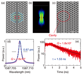
This phenomenon (negative refraction) in photonic crystals was first discovered by our group in 2000 [2]. We found that strongly modulated photonic crystals can exhibit negative refraction in the vicinity of the photonic bandgaps, and we demonstrated it by numerical simulation of electromagnetic wave propagation in realistic photonic crystals. The calculated light propagation in a two-dimensional hexagonal pillar GaAs photonic crystal obtained by the finite-difference time-domain method is illustrated in Fig. 2(b). We also found that negative refraction produces various unconventional light propagation phenomena. One such example is shown in Fig. 2(c), where the light generated from a point source is converged in a negative-index photonic crystal. This shows that a flat surface of a negative-index material can act like a lens. Furthermore, this flat lens is very different from a conventional lens because it has neither a specific focal length nor a principal axis. In a sense, this negative-index lens is similar to a mirror. A mirror generally produces a virtual mirror-inverted image on the opposite side of the mirror boundary, but the negative-index lens produces a real mirror-inverted image in the negative-index material. It is easily understood that negative refraction occurs twice when there are two boundaries, so a slab of negative-index material can produce a real image on the other side of the air region (negative-index slab lens). The appearance of negative refraction is related to the negative curvature of some bands in Fig. 1(c). If dω/dk is negative, the group velocity (vg = dω/dk) has the opposite sign to the wavevector (k). If one applies wavevector conservation at the boundary interface, the direction of the group velocity should be negative. However, the negative sign of the group velocity is not the only requirement for this phenomenon. To have a meaningful refractive index given by Eq. (1), it is essential to have an isotropic group velocity. In fact, a negative group velocity can be achieved in conventional diffraction gratings, but they cannot produce negative refraction because the negative value of the group velocity shows up only at a certain incidence angle. We found that an isotropic negative group velocity can appear in the vicinity of strongly modulated photonic crystals. In this condition, one can define a simple negative index value irrespective of the incidence angle, which eventually produces the beautiful focusing shown in Fig. 2(c). After our prediction, numerous experimental verifications were reported, first in the microwave region and later in the optical frequency region. This concept was later generalized to other wave phenomena, including surface fluidic waves, acoustic waves, and electron waves. Currently, many research groups are studying these phenomena with the aim of making new imaging systems. In an amazing example of the synchronicity of science, at almost the same time as our paper’s publication, a similar phenomenon was reported in radio-frequency metal metamaterials (so-called left-handed materials), which rely on a totally different mechanism. Negative-index materials are now one of the important hot topics in research on electromagnetic waves. 3. Strong light confinement in photonic crystals and all-optical memoriesNext, I will show how photonic crystals are powerful in terms of light confinement. Light confinement is one of the most important targets in photonics because the generally poor light confinement in conventional optic media or devices hampers the miniaturization and integration of photonic devices. In addition, the generally weak light-matter interaction is enhanced by strong light confinement. These characteristics could potentially overcome the weak points of photonics technologies in comparison with electronics technologies. The target here is equivalent to achieving a high quality-factor (Q) and small optical resonators (cavities). Light confinement in a cavity generally becomes exceedingly difficult as the cavity size becomes small. Since light is confined by multiple reflections, the required number of reflections becomes increasingly larger for smaller cavities. For example, if the target is to confine photons for 1 ns in a 1-µm3 volume, the required number of reflections is around 300,000, which means that the reflectivity should be higher than 99.999%. Such high reflectivity cannot be achieved by metal mirrors. Total internal reflection, which occurs at the refractive index boundary, can theoretically be 100%, but this is true only for large cavities. When the cavity size is comparable to the optical wavelength, the total internal reflection condition breaks down because of wavevector broadening. As mentioned in the introduction, the photonic bandgap can resolve this problem because we can prevent the escape of light by placing photonic bandgap materials (photonic insulators), without inducing absorption. This idea was proposed two decades ago [3], but ultrahigh-Q wavelength-sized cavities have been made only within the last couple of years, by using high-quality photonic crystals. Figure 3(a) shows an ultrahigh-Q design of an optical cavity in the two-dimensional photonic crystal shown in Fig. 1(a) [4]. Contrary to the original proposal, the strong light confinement was achieved not in three-dimensional (3D) photonic bandgap materials, but in two-dimensional (2D) ones. This is because 2D ones can be fabricated very precisely thanks to the rapid progress of CMOS fabrication technologies. Of course, the bandgap confinement cannot be perfect in 2D systems, but researchers have finally found several ways to optimize the confinement produced by 2D bandgaps. In the case in Fig. 3(a), the cavity is based on a line-defect waveguide, which is theoretically loss-free. If this waveguide were simply terminated, the termination would deform the original loss-free mode profile, which would eventually produce substantial out-of-plane radiation loss. In our case, the waveguide is not terminated: instead, we slightly shift the position of some of air holes, as shown in the plot. The shift is as small as a few nanometers, which does not alter the original loss-free mode profile. We have found that such a small shift is sufficient to create the strongly confined cavity mode shown in Fig. 3(b). A numerical calculation shows that the theoretical cavity Q is over 108 and the cavity mode volume is as small as 1.5(λ/n)3 (λ: resonance wavelength). A scanning electron microscope image of the cavity is shown in Fig. 3(c).
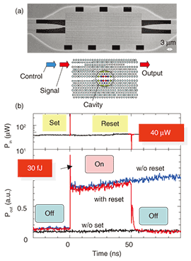
Our recent measurements of ultrahigh-Q cavities fabricated in silicon photonic crystal slabs are shown in Figs. 3(d) and (e). The transmission spectrum (Fig. 3(d)) shows a sharp resonance peak, whose width corresponds to a cavity Q of 1.8 ×10⁶. The decay time of a light pulse in the cavity, independently measured for the same device (Fig. 3(e)), was 1.53 ns, which corresponds to exactly the same Q. These results directly show that well-designed photonic crystals can confine photons for over 1 ns within a wavelength-sized volume [5], which has not been achieved by anything other than photonic crystals. Extensive studies on microcavities are currently being conducted using various methods. Among them, photonic crystals are showing outstanding performance in terms of the strong light confinement within a wavelength-sized volume, which must be advantageous for the dense integration of photonic devices and enhancement of light-matter interaction. We are currently pursuing the possibility of ultrahigh-Q photonic crystal cavities for application to an all-optical memory [6]. Although all-optical memories have a long research history, their performance is still limited. They are too large, difficult to integrate, and require too much energy. Photonic crystal cavities seem to be advantageous for the first and second issues. Concerning the third issue, the enhancement of light-matter interaction in high-Q and small cavities should be advantageous. It is well known that a cavity with optical nonlinearity exhibits bistable action, which can be used as an optical memory. The energy efficiency of this operation scales as Q/V (V: cavity mode volume). This means that we can expect a significant reduction in the driving energy for optical memories. A schematic of our device, which consists of a width-modulated line-defect cavity and input/output waveguides based on an InGaAsP photonic crystal [7], is shown in Fig. 4(a). In this device, the output intensity of a signal light (resonant to one of the cavity modes) is modulated by injecting another control light (also resonant to another cavity mode) into the cavity because the control light shifts the cavity mode via the optical nonlinearity of InGaAsP. More precisely, carriers are generated by a two-photon absorption process in the InGaAsP cavity, and the refractive index of the cavity shifts as a result of carrier-plasma dispersion. Such a nonlinear resonator switch is known to exhibit bistable behavior above a certain threshold power. The bistable switching operation (bit memory operation), in which set and reset pulses change the output state between the on and off states, is shown in Fig. 4(b). Note that the driving power for this memory is as low as 40 μW, which is approximately two orders of magnitude smaller than the power required for other types of optical memories. This power reduction is primarily due to the light-matter interaction enhancement in high-Q nanocavities. Since cavities of this type are suitable for dense integration in a chip, we expect them to be promising for making photonic random access memory. We are currently working on integrating many memories in a chip.
As regards the light confinement, we have recently found that strong light confinement can also be achieved in other type of structures. For example, a certain type of photonic amorphous structure can have large 3D photonic bandgaps with strong light confinement [8]. 4. Slow light in photonic crystalsAs described in the introduction, controlling the speed of light in media is a very important issue. This is especially true for slowing light down because slow light will enable optical buffering, which is a difficult function to achieve with conventional photonics technologies. In addition, light-matter interaction is generally enhanced in slow-light modes because the spatial length of an optical pulse is compressed and the interaction time becomes longer. As discussed in section 2, photonic crystals can greatly alter the group velocity (vg = dω/dk) by photonic band formation. Therefore, one would expect a significant reduction in the light speed. We experimentally demonstrated this superior performance of photonic crystals as slow-light waveguides in the early stage of our photonic crystal studies. Figure 5(a) shows the dispersion of a single line-defect waveguide in a hexagonal air-hole photonic crystal in Si (depicted in the inset of Fig. 5(b)). We paid attention to a waveguiding mode located within the photonic bandgap, whose slope (dω/dk) decreases as the frequency approaches the band edge. (This tendency generally appears in the vicinity of the photonic band edge and is sometimes referred to as “band-edge slow light”) In 2001, we measured the group refractive index (ng) of photonic crystal waveguides of this type as a function of the incident wavelength [9]. The results are shown in Fig. 5(b), which clearly demonstrates that the speed of light is reduced to c/90 because vg = c/ng. At that time, slow light had been observed only in ultracold atomic gas, and our report was the first demonstration of slow light in dielectric systems. Atomic gaseous systems are unsuitable for on-chip device integration, so our demonstration showed the possibility of slow-light manipulation in a semiconductor chip.
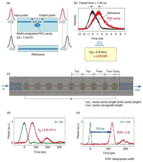
However, the band-edge slow-light mode in Fig. 5(a) has an intrinsic drawback. In this dispersion, as vg becomes smaller, the group velocity dispersion also becomes larger. That is, a slow-light pulse in a waveguide of this type should be seriously affected by pulse broadening. To avoid this, we must be more careful in designing the dispersion. Extensive studies are currently underway to achieve desirable dispersion in photonic crystal waveguides having sophisticated designs. For example, we have also reported slow-light pulse transmission in coupled waveguides of a certain type [10]. There is another way to achieve dispersion-managed slow-light modes: we can use a resonator. A resonator generally induces a group delay of 2τ (τ : cavity’s photon lifetime = Q/ω0) at the resonance frequency. In addition, the pulse transit speed across the cavity should roughly scale with the cavity size. Most importantly, the group velocity dispersion is always zero at the resonance frequency. Hence, small and high-Q cavities should generate dispersion-free slow light. In this scenario, the ultrahigh-Q nanocavities mentioned in the previous section are ideally suitable. From this reason, we are now focusing on cavity-based slow light produced using photonic crystals. Figures 6(a) and (b) shows a slow-light pulse propagation experiment for ultrahigh-Q nanocavities in photonic crystals. The cavity design is the same as in Figs. 3(a) and (c). We observed an optical delay of 1.53 ns, which is comparable to the cavity lifetime. From this value, we estimated the pulse transit speed to be 5800 m/s, which corresponds to c/50,000. This extreme reduction in light speed is primarily due to the ultrahigh-Q value and small size of our cavity. As far as we know, this is the lowest light speed ever achieved in all-dielectric systems.
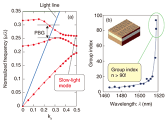
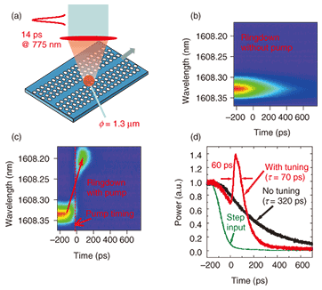
For practical application of cavity-based slow light, coupled cavity waveguides have been considered as the best manifestation. In terms of group velocity, a single cavity would have the lowest value, but the bandwidth is directly linked to its delay. On the other hand, coupled waveguides can have a longer delay or wider bandwidth depending on the structure parameters. There had been various trials to achieve slow-light modes in coupled cavity waveguides based on microspheres or microring cavities, but the performance was limited because of their poor Q values and large cavity size. We have recently been successful in making large-scale arrays (Nmax = 200, where N is the number of cavities) of ultrahigh-Q nanocavities, as shown in Fig. 6(c), which was the first demonstration of large-scale coupled cavities based on wavelength-sized resonators [11]. The cavity design is the same as in Fig. 3(a), and we experimentally confirmed that the cavity array exhibited an overall Q of ˜106. We observed considerably high transmittance (>50%) even for N = 200 samples, which means that 200 ultrahigh-Q cavities are coherently coupled to each other (otherwise there would be no transmission). We directly observed slow-light pulse propagation with a group velocity as low as c/170 (Fig. 6(d). This is the lowest reported value for all-dielectric slow-light waveguides. In contrast with the single-cavity result, the achieved delay was six times longer than the output pulse width (Fig. 6(e)). This is because the delay is not limited by the bandwidth. 5. Novel way of manipulating lightAs discussed in the introduction, the ways of manipulating light are limited in comparison with the ways of manipulating electrons. In electronic circuits or devices, the states of electrons can be easily controlled by applying voltage, which changes the kinetic energy of electrons directly. This explains how various electronic devices work. On the other hand, the energy (equivalently, frequency) of photons cannot be easily changed. Obviously, photons are not affected by voltage or any potential energy. In other words, photons cannot be accelerated or decelerated by directly affecting their kinetic energy. Thus, the frequency of photons running within a photonic circuit is constant once the photons have been generated. The ultrahigh-Q nanocavities and slow-light media discussed in sections 3 and 4 can change this paradigm. If photons can be stored in a microcavity (or slow-light medium) for a sufficiently long time, we can directly change their state by changing some parameters of the cavity (or waveguide). This process is equivalent to tuning a guitar. Suppose you pluck a guitar string to generate a sound with tone C. You can easily change the tone (for example, to F) by turning the tuning peg before the sound dies out. This is called adiabatic parameter tuning of a classical oscillation. You can do basically the same thing for light (which is an electromagnetic oscillation), though it is normally very difficult because light passes by and decays very fast. Ultrahigh-Q nanocavities and slow-light media provide us with a novel tuning mechanism. In 2006, we predicted that it would be possible to dynamically change the wavelength of photons captured in a cavity by rapidly changing the cavity’s resonance wavelength [12]. We termed this process adiabatic wavelength conversion. Note that conventional wavelength conversion processes using optical nonlinear materials, such as second-harmonic generation or optical parametric conversion, are totally different phenomena. Such conventional conversion processes do not conserve the total number of photons: photons are merged or divided to generate a new frequency component. In the adiabatic conversion process, the photon number does not change, and a certain amount of energy is directly given to or taken from each photon. Very recently, we clearly observed this phenomenon in an ultrahigh-Q nanocavity in a silicon photonic crystal, as shown in Fig. 7 [13]. The cavity structure (Fig. 7(a)) is similar to that in section 3. First, we injected light into the cavity from the waveguide, and then we abruptly switched off the input. Before the stored light leaked out from the cavity, we delivered another light pulse from the top surface and this changed the cavity’s resonance wavelength (similar to what we did in the optical switching action in section 3). Time-resolved spectra with and without a tuning pulse are shown in Figs. 7(b) and (c). Without tuning, the whole spectrum decayed without changing its shape. With tuning, the spectrum abruptly shifted to the shorter wavelength, which demonstrates the adiabatic wavelength conversion of light in the cavity.
In the course of the process in Fig. 7(c), we directly altered the frequency of photons in the cavity, which is analogous to the voltage control of electrons in electronic devices. This analogy led us to consider possible device operation based on this tuning. As described in Fig. 3(a), this cavity mode is formed by very slight structural modulation. Hence, the confinement should be very sensitive to the frequency of photons. If we adiabatically raise the frequency of photons, the confinement becomes weaker in such a way that the trapped photons are extracted to the waveguide. We directly observed this phenomenon, in which a short pulse was generated after the tuning. The results are shown in Fig. 7(d). Note that the pulse width was much shorter than the original cavity’s photon lifetime. This operation is somewhat similar to the operation of a charge-coupled device in which electrons are transferred by the manipulation of the electric potential. We believe that this tuning mechanism will make possible various novel functions that are difficult for photonics technologies. The adiabatic tuning of photons could also lead to various other intriguing physical processes. We have clarified that it can be used to dynamically stop photons [14], [15]. As another unique example, we have clarified that optomechanical energy conversion (between light and mechanical movement) can be extremely efficient when adiabatic wavelength conversion is used for cavities having movable parts [16], which will be useful for making super-efficient optical microelectromechanical systems or optical tweezers. 6. OutlookIn this article, I have shown that photonic crystals enable various novel ways of manipulating light in media beyond the limitations for conventional materials found in nature. The exotic dispersion of photonic band structures is used to generate enigmatic negative-index states and achieve extreme slow-light modes. The existence of photonic bandgaps also creates strong light confinement in wavelength-sized ultrahigh-Q cavities, which enables the energy consumption of optical devices to be reduced enormously. In addition, dynamical tuning of high-Q nanocavities or slow-light media produces unique novel functions that have not been considered in conventional photonics. To fully enjoy the intrinsic superior advantages of photonics over electronics, we must break through the limitations of current photonics technologies. In this respect, photonic crystals are showing their potential to resolve these issues. By using photonic crystals, one can tightly squeeze an optical pulse within a wavelength-sized cavity and dynamically control the speed of the light pulse. These low-energy light pulses can perform various functions. Furthermore, all of these features can be achieved on a single tiny chip. Although we may have to overcome various technological problems, photonic crystals are definitely promising for making photonics play a more functional and intelligent role in information processing. References
|
||||||||||||||||||||||||||||||||||||